
 Released:2026-01-09 15:52:19
 Views 850 次
 在工业控制、环境与气体传感、便携式仪表及嵌入式终端等应用场景中,模拟信号链长期处于一种稳定却受限的工程环境:供电电压持续向低压与单电源方向集中,系统功耗预算愈发紧张,信号频率和精度需求维持在中低水平,然而对系统稳定性、抗干扰能力以及量产一致性的要求却不断提高。CBM6001正是针对这一系列情况推出的一款CMOS单通道运算放大器,其设计目标是为中低频、低功耗、规模化应用提供可预期且易落地的模拟放大方案。

In industrial control, environmental and gas sensing, portable instrumentation, and embedded terminal applications, analog signal chains operate in a stable yet constrained engineering environment. Power supply voltages increasingly concentrate at low levels and single-supply configurations, while system power budgets become increasingly tight. Requirements for signal frequency and precision remain at medium-low levels, yet demands for system stability, anti-interference capability, and mass production consistency continue to rise. The CBM6001 is a CMOS single-channel operational amplifier specifically designed to address these challenges. Its design objective is to provide a reliable and practical analog amplification solution for medium-low frequency, low-power, and scalable applications.
1. Power Supply and Power Consumption: Basic Capabilities for Power Limited Systems
The CBM6001 supports a wide voltage range from 2.1V to 6.0V, covering mainstream power supply architectures including single-cell lithium batteries and 3.3V/5V industrial power supplies. Within this range, its typical static current per channel is only 80µA.
The engineering significance of this power consumption level lies in:
l It can significantly reduce the power consumption ratio of the analog front-end in multi-channel systems.
l Free up energy budget for high-power units like MCUs and wireless modules
l Designed for systems requiring prolonged power supply or extended standby operation
The device also delivers a peak power supply rejection ratio (PSRR) of 100dB, which significantly reduces reliance on external power filtering and isolation designs in systems with pronounced power ripple and load disturbances.
II. Input Characteristics: High Impedance and Real Ground Inductance
The CBM6001 features a CMOS input architecture with pA-level bias current, enabling direct interfacing with high-impedance signals to minimize system errors caused by input bias.
Its input common-mode voltage range covers and slightly exceeds the power rail (approximately ±100mV), delivering two direct engineering benefits:
1. Supports true ground potential sensing without requiring an additional negative power supply
2. The system can still process input signals near the power rail completely under low-voltage power supply conditions.
In terms of performance, the CBM6001 demonstrates a typical input offset voltage of ±0.5mV and a temperature drift of 2µV/°C. This configuration is ideal for general-purpose measurement and control systems requiring mV-level precision without zero drift architecture, achieving a balanced trade-off between cost, power consumption, and accuracy.
III. Dynamic Performance: Controllable Bandwidth for Low and Medium Frequency Closed-loop Applications
The CBM6001 features a gain-bandwidth product of 1MHz and a slew rate of 0.7V/µs. From a system design perspective, this performance combination clearly indicates:
l low and medium frequency signal conditioning
l active filtering
l Application of Buffer and Amplifier
Under typical closed-loop gain conditions, the CBM6001 delivers predictable frequency response and phase margin (typically 60°), which helps shorten stability verification cycles and reduce the design complexity of compensation networks.
This parameter orientation does not pursue high speed, but defines clear boundaries for system design that prioritizes broad application coverage and stability, enabling engineers to quickly assess its suitability during the selection phase.
IV. Output Capability: Track-to-Track Output and Load Adaptability
The CBM6001 features a rail-to-rail output architecture that delivers an output swing approaching the power rail under 10kΩ load conditions, with typical values of 3mV and a maximum of 15mV. This capability is particularly critical in low-voltage systems, enabling:
l Enhance the ADC's available input dynamic range
l Reduce the system's dependence on additional voltage boosting or bias circuits
The device features an output short-circuit current capacity exceeding 100mA, with its driving characteristics for capacitive loads explicitly detailed in the parameter manual. In high-capacitance load scenarios, engineering controllable trade-offs between stability and response speed can be achieved through proper configuration of output series resistance.
V. Noise and Distortion: Meeting the General Signal Quality Requirements
In terms of noise performance, the CBM6001 features an input voltage noise density of 27 nV/√Hz (1 kHz) and low-frequency noise (0.1Hz to 10 Hz) of 8 µVpp. These specifications align with the typical characteristics of low-power CMOS operational amplifiers, making it suitable for most sensor interfaces and control signal conditioning applications.
At 1kHz, unit gain, and 2kΩ load, the total harmonic distortion plus noise (THD+N) is 0.003%. This performance indicates the device maintains high fidelity and signal purity, meeting the distortion control requirements of standard analog signal chains.
VI. Packaging and Reliability: For Mass Production and Environmental Adaptability
The CBM6001 supports mainstream packaging types including SOT23-5, SOP-8, and SC70-5, effectively meeting the design requirements of both high-density PCBs and conventional industrial boards. With an operating temperature range of-40°C to +125°C and storage temperature capacity of-65°C to +150°C, it is designed for long-term operation in industrial and automotive-grade environments.
Typical application scenarios
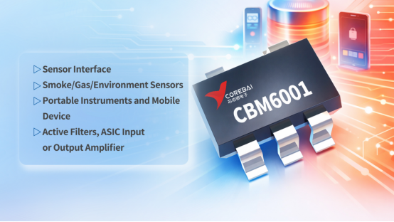
The CBM6001 is widely applicable to various general analog front-end applications, including but not limited to:
In the field of industrial and environmental monitoring, it is used for buffering and amplifying sensor signals such as temperature, gas, and pressure.
It is used as a low power analog signal conditioning unit in portable instrument and battery power supply equipment.
In embedded systems, it functions as an ADC input stage, a DAC output buffer, or a simple active filter circuit.
It provides stable and predictable general-purpose operational amplification in consumer and industrial control products.
010-62106066
( Monday to Friday 9:00 - 18:00 )
 704-705, Block D, Building 2, No. 9 Fenghao East Road, Haidian District, Beijing

Wechat Public Account

This app respects and protects the privacy of all users who use the service. In order to provide you with more accurate and personalized services, this app will use and disclose your personal information in accordance with this Privacy Policy. However, this application will treat this information with a high degree of diligence and prudence. Except as otherwise provided in this Privacy Policy, this application will not disclose or provide this information to third parties without your prior permission. This app will update this privacy policy from time to time. By agreeing to this Application Services Use Agreement, you are deemed to have agreed to the entire content of this Privacy Policy. This Privacy Policy is an integral part of this Application Service Agreement.
 A/D Converters (ADC)
 RF Transceiver
 Controller
 Power Management
 Logic gates
 Real-time clocks
 Digital Isolator
 Darlington Transistor
 D/A Converters (DAC)
 Sensors
 Analog Switches Multiplexers
 Interface
 Monitoring Circuit
 Amplifier
 在线商城
在线商城