 Released:2026-01-28 16:54:08
 Views 369 次
 在当前工业自动化、高端医疗成像及无线通信系统向多通道、大带宽演进的背景下,信号链前端的模数转换器(ADC)正面临着精度、功耗与同步复杂性的三重挑战。芯佰微电子推出的CBM96AD56是一款专门针对低功耗、小尺寸和使用灵活性开发的四通道、16位、125MSPS模数转换器。该器件通过集成高性能架构与JESD204B Subclass 1 高速串行接口,为复杂信号链提供了高可靠性的底层支撑。

In the context of industrial automation, advanced medical imaging, and wireless communication systems evolving toward multi-channel and high-bandwidth architectures, analog-to-digital converters (ADCs) at the signal chain front-end face triple challenges: precision, power consumption, and synchronization complexity. Corebai Microelectronics' CBM96AD56 is a 4-channel, 16-bit, 125MSPS ADC specifically designed for low power consumption, compact size, and operational flexibility. By integrating a high-performance architecture with the JESD204B Subclass 1 high-speed serial interface, this device provides a highly reliable foundation for complex signal chains.

In precision signal acquisition systems, baseline noise control and linearity directly determine the system's effective resolution. The CBM96AD56 employs a multi-stage pipeline architecture, with redundancy bits configured at each stage to eliminate comparator offset errors.
(1) Signal-to-noise ratio (SNR) performance: Under 9.7MHz input and 1.4V reference voltage, the device delivers a typical SNR of 79 dBFS. For applications such as medical ultrasound imaging, this translates to enhanced image contrast and precise extraction of weak echo signals.
(2) Spurious Free Dynamic Range (SFDR): The typical range spans from 85dBc to 91dBc. High SFDR enables multi-carrier receivers to effectively distinguish between strong adjacent-frequency interference and weak target signals, thereby reducing the design complexity of front-end filters.
(3) Linearity assurance: The differential nonlinearity (DNL) is ±0.6LSB, and the integral nonlinearity (INL) is ±5.0LSB. Stable linearity ensures continuous data conversion and prevents quantization distortion under large dynamic ranges.
The CBM96AD56 features a full-power analog input bandwidth of 650MHz, delivering substantial implementation value at the system architecture level.
(1) Simplified RF front-end: Broadband input support enables engineers to implement intermediate frequency (IF) sampling in radar detection or wireless communication systems. By directly capturing high-frequency signals, the number of mixing stages can be reduced, lowering overall bill of materials (BOM) costs and shrinking PCB dimensions.
(2) Input matching optimization: The device's analog input employs a differential switch-capacitor circuit, supporting a wide common-mode range. Designers can utilize low-Q inductors or ferrite beads to reduce the high differential capacitance at the analog input, achieving optimal performance in high and medium frequency environments.
For large-scale phased array radars or multi-antenna base stations, phase alignment between multi-chip sampling is the core challenge in design. The CBM96AD56 employs the JESD204B Subclass 1 protocol to address deterministic delay issues at the foundational level.
(1) Three-phase synchronization logic: The device establishes a stable link through three phases: Code Group Synchronization (CGS), Initial Channel Alignment Sequence (ILAS), and data transmission.
(2) Deterministic delay control: By utilizing the SYSREF and DSYNC signals, the system achieves precise alignment of local multi-frame clock (LMFC). The SYSREF edge not only generates the internal LMFC signal but also resets the ADC sampling edge, ensuring complete synchronization of sampling instances across multiple devices.
(3) Cabling and Scalability: Each channel supports up to 8.0Gbps, significantly reducing the number of connections between ADC and FPGA. The JESD204B module offers 1/2/4 channel configurations, enabling users to flexibly map data paths based on the throughput requirements of downstream logic resources.
In portable measurement and high-density module design, thermal management directly impacts device lifespan. The CBM96AD56 achieves high performance while maintaining precise power consumption balance.
(1) High power efficiency: In 125MSPS operation mode, the power consumption per channel is ≤195mW.
(2) Smart Power Mode:
l Complete power-off mode: consumes under 14mW, ideal for portable devices with extreme battery life requirements.
l Standby mode: With a typical power consumption of 547mW, the internal reference voltage circuit remains powered, enabling a rapid wake-up time of approximately 250ns. This ensures the system can seamlessly switch between energy efficiency and fast response.
(3) Calibration and Stability: The built-in duty cycle stabilizer (DCS) automatically corrects clock duty cycle deviations, ensuring dynamic performance even with non-standard clock sources.
(1) Industrial-grade environmental adaptability: The device operates within a rated temperature range of-40°C to +85°C, meeting the deployment requirements of harsh industrial environments.
(2) SPI deep configuration: Engineers can fine-tune offset adjustment (address 0x10), input range selection (address 0x18), and output driver level (address 0x15) through the three-wire SPI interface.
(3) Thermal design: The device features a 56-pin QFN package (8mmx8mm). The manual explicitly recommends connecting the exposed bottom pad to analog ground (AGND), with multiple thermal vias on the PCB providing low-thermal-resistance paths to ensure electrical stability during high-speed operation.
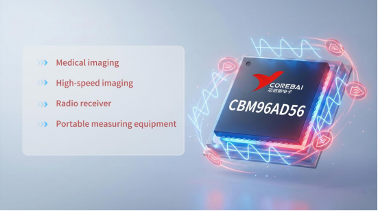
application area
(1) In medical imaging, the four-channel synchronous acquisition and high SNR ratio meet the signal collection requirements of ultrasound probe arrays, while the compact packaging and low-power design facilitate the miniaturization of portable ultrasound devices.
(2) In the field of communication RF, the JESD204B interface with multi-chip synchronization capability is designed for 5G base station multi-antenna receiving systems, where its wide bandwidth and high Signal-to-Noise Ratio (SFDR) ensures precise demodulation of RF signals.
(3) In the industrial and testing fields, the flexible input range and testing modes can meet the multi-scenario signal acquisition needs of high-speed industrial cameras, handheld oscilloscopes, and other devices, while reducing their size and power consumption.
010-62106066
( Monday to Friday 9:00 - 18:00 )
 704-705, Block D, Building 2, No. 9 Fenghao East Road, Haidian District, Beijing

Wechat Public Account