
 Released:2023-04-17 09:25:05
 Views 2921 次
 CMOS, Low Voltage, Low On-Resistance, Low On-Resistance Flatness, Low Power Consumption, Quad-Channel

CMOS, Low Voltage, Low On-Resistance, Low On-Resistance Flatness, Low Power Consumption, Quad-Channel
The CBMG711, CBMG712, and CBMG713 are monolithic CMOS devices containing four independently selectable switches. These switches are designed on an advanced submicron process that provides low power dissipation yet gives high switching speed, low on resistance, low leakage currents, and high bandwidth.
They are designed to operate from a single 1.8 V to 5.5 V supply, making them ideal for use in battery-powered instruments and with the new generation of DACs and ADCs from Corebai. Fast switching times and high bandwidth make the parts suitable for switching USB 1.1 data signals and video signals.
The CBMG711, CBMG712, and CBMG713 contain four independent single-pole/single-throw (SPST) switches. The CBMG711 and CBMG712 differ only in that the digital control logic is inverted. The CBMG711 switches are turned on with a logic low on the appropriate control input, while a logic high is required to turn on the switches of the CBMG712. The CBMG713 contains two switches whose digital control logic is similar to the CBMG711, while the logic is inverted on the other two switches,please refer to the product function block diagram Figure 2 for details.
Each switch conducts equally well in both directions when On. The CBMG713 exhibits break-before-make switching action.
The CBMG711/CBMG712/CBMG713 are available in 16-lead TSSOP and 16-lead SOP packages.
functional block diagram
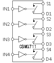
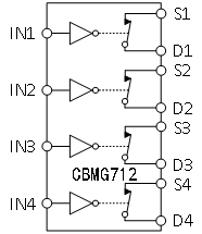
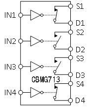
Figure 1 shows a switch displaying a logic input of “1”.
Table 1. Truth Table (CBMG711/CBMG712)
|
CBMG711 In |
CBMG712 In |
Switch Condition |
|
0 |
1 |
ON |
|
1 |
0 |
OFF |
Table 2. Truth table(CBMG713)
|
Logic |
Switch 1,4 |
Switch 2,3 |
|
0 |
OFF |
ON |
|
1 |
ON |
OFF |
Typical features
1.8 V to 5.5 V single supply
Low on resistance (2Ω Typ) at VDD=5.5V
Low on resistance flatness(0.3Ω Typ)at VDD=5.5V
−3 dB bandwidth > 200 MHz
Rail-to-rail operation
16-lead TSSOP and SOP packages
Fast switching times: tON = 16 ns tOFF = 10 ns
Typical power consumption: (< 0.01 μW)
TTL/CMOS compatible
Product Application
Cell phones
Video switching
Communication systems
Battery-powered systems
USB 1.1 signal switching circuits
Mechanical reed relay replacement
Product highlight
1.1.8 V to 5.5 V Single-Supply Operation. The CBMG711, CBMG712, and CBMG713 offer high performance and are fully specified and guaranteed with 3V and 5V supply rails.
2. Very Low RON (4.5Ω maximum at 5 V, 8Ω maximum at 3V). At supply voltage of 1.8V, RON is typically 35Ω over the temperature range.
3. Low On Resistance Flatness.
4. −3dB Bandwidth >200 MHz.
5. Low Power Dissipation. CMOS construction ensures low power dissipation.
6. Fast tON/tOFF.
7. Break-Before-Make Switching. This prevents channel shorting when the switches are configured as a multiplexer (CBMG713 only).
8. 16-Lead TSSOP and 16-Lead SOP Packages.
Electrical characteristic diagram
The diagrams of several main parameters of CBMG711/CBMG712/CBMG713 are as follows:
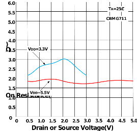
Figure 2.On Resistance vs. VD (VS)-(CBMG711)
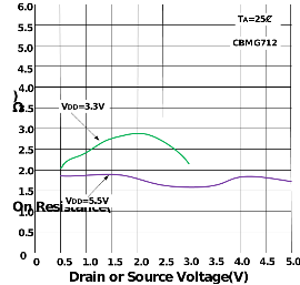
Figure 3.On Resistance vs. VD (VS)-(CBMG712)
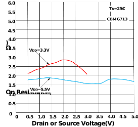
Figure 4.On Resistance vs. VD (VS)-(CBMG713)
————END————

http://www.corebai.com/

010-62106066
( Monday to Friday 9:00 - 18:00 )
 704-705, Block D, Building 2, No. 9 Fenghao East Road, Haidian District, Beijing

Wechat Public Account

This app respects and protects the privacy of all users who use the service. In order to provide you with more accurate and personalized services, this app will use and disclose your personal information in accordance with this Privacy Policy. However, this application will treat this information with a high degree of diligence and prudence. Except as otherwise provided in this Privacy Policy, this application will not disclose or provide this information to third parties without your prior permission. This app will update this privacy policy from time to time. By agreeing to this Application Services Use Agreement, you are deemed to have agreed to the entire content of this Privacy Policy. This Privacy Policy is an integral part of this Application Service Agreement.
 A/D Converters (ADC)
 RF Transceiver
 Controller
 Power Management
 Logic gates
 Real-time clocks
 Digital Isolator
 Darlington Transistor
 D/A Converters (DAC)
 Sensors
 Analog Switches Multiplexers
 Interface
 Monitoring Circuit
 Amplifier
 在线商城
在线商城