
 Released:2023-10-16 02:10:13
 Views 5231 次
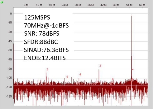
 CBM16AD125 is a dual channel, 16 bit, 125MSPS analog-to-digital converter (ADC) that supports multifunctional communication applications that require high performance, low cost, and small size. This dual channel ADC core adopts a multi-level differential pipeline architecture, and each ADC integrates a high bandwidth differential sampling and holding circuit, supporting various input ranges that users can choose from. The chip integrates a reference voltage source internally, making it easy to simplify external design. The duty cycle stabilizer can be used to compensate for changes in the ADC clock duty cycle, ensuring excellent performance of the converter. ADC output data can be directly sent to two external 16 bit output ports, supporting two modes: 1.8VCMOS and LVDS. Flexible power-off options can significantly reduce power consumption. The three wire SPI compatible serial interface can configure various functions of the product. CBM16AD125 adopts a 64 pin QFN package, with a rated temperature range of -40 ℃ to+85 ℃ industrial temperature.

new products
Keywords: 16 bit, dual channel, 1.8V, high-speed ADC, low power consumption
Functional Block Diagram

Figure 1 Functional Block Diagram
Typical features
Product application
Radar system
Diversity Radio System
Multimode Digital Receiver (3G)
GSM/EDGE/W-CDMA/LTE/CDA2000 WiMAX/TD-SCDMA
I/O demodulation system
Smart antenna system
General Software Radio
Broadband data applications
Ultrasound equipment
Core features
Compatible with AD9258/AD9268 pins, 16 bit products can be easily converted to 14 bit products.
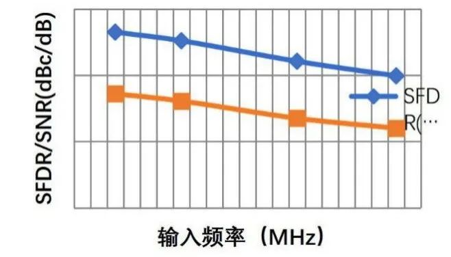
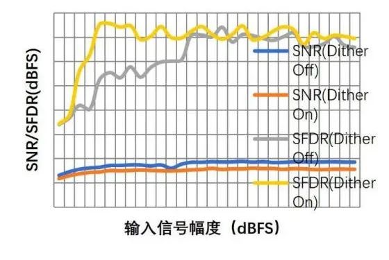
Typical electrical characteristic diagram

010-62106066
( Monday to Friday 9:00 - 18:00 )
 704-705, Block D, Building 2, No. 9 Fenghao East Road, Haidian District, Beijing

Wechat Public Account

This app respects and protects the privacy of all users who use the service. In order to provide you with more accurate and personalized services, this app will use and disclose your personal information in accordance with this Privacy Policy. However, this application will treat this information with a high degree of diligence and prudence. Except as otherwise provided in this Privacy Policy, this application will not disclose or provide this information to third parties without your prior permission. This app will update this privacy policy from time to time. By agreeing to this Application Services Use Agreement, you are deemed to have agreed to the entire content of this Privacy Policy. This Privacy Policy is an integral part of this Application Service Agreement.
 A/D Converters (ADC)
 RF Transceiver
 Controller
 Power Management
 Logic gates
 Real-time clocks
 Digital Isolator
 Darlington Transistor
 D/A Converters (DAC)
 Sensors
 Analog Switches Multiplexers
 Interface
 Monitoring Circuit
 Amplifier
 在线商城
在线商城