 Released:2021-10-28 00:00:20
 Views 2467 次
 The CBMG719 is a single-pole double-throw (SPDT) CMOS switch. It operates within a single supply voltage range of 1.8 V to 5.5 V, making it highly suitable for battery-powered instruments and applications in conjunction with DACs and ADCs.

The CBMG719 is a single-pole double-throw (SPDT) CMOS switch. It operates within a single supply voltage range of 1.8 V to 5.5 V, making it highly suitable for battery-powered instruments and applications in conjunction with DACs and ADCs.
CBMG719 Functional Diagram
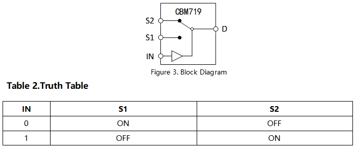
IN serves as the digital switch enable, thereby controlling switches S1 and S2. Hereunder is the functional block diagram and truth table for the CBMG719:

CBMG719 Typical Features
l 1.8 V to 5.5 V single supply
l 2.5 Ω (typ) on resistance
l 0.75 Ω (typ) on resistance flatness
l −3 dB bandwidth > 200 MHz
l Rail-to-rail operation
l 8-Lead SOP package
l Fast switching times: tON = 12 ns tOFF = 6 ns
l Typical power consumption: (< 0.01 μW)
l TTL/CMOS compatible
CBMG719 Product Highlights
● The CBMG719 switch features low power consumption, fast switching speed, low on-resistance, and small leakage current.
● Each switch within the CBMG719 exhibits identical conduction performance in both directions when turned on. The CBMG719 is of the break-before-make type. Additionally, the device can achieve a −3 dB bandwidth greater than 200 MHz.
● The chip functions normally across a temperature range from -40°C to +125°C, demonstrating a certain level of reliability.
CBMG719Typical Electrical Characteristics Diagram
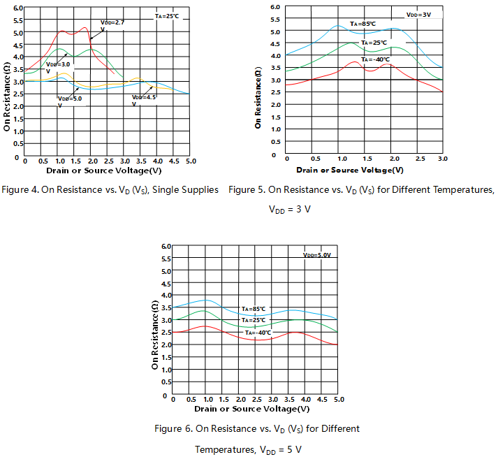
CBMG719 Graphs of Several Key Parameter Characteristics as follows:

010-62106066
( Monday to Friday 9:00 - 18:00 )
 704-705, Block D, Building 2, No. 9 Fenghao East Road, Haidian District, Beijing

Wechat Public Account