
 Released:2025-11-13 10:14:55
 Views 1251 次
 在工业传感、便携电子、精密检测等领域,μV~mV级微弱信号采集始终面临“高性能、低功耗、低设计复杂度”的矛盾。具体而言,传统分立器件方案需搭配PGA放大、滤波、ADC等多模块,这不仅导致信号链路冗长、噪声引入多,还推高了研发难度与BOM成本;而通用ADC芯片则难以同时满足高输入阻抗、低功耗与小体积的核心需求。

In fields such as industrial sensing, portable electronics, and precision measurement, the acquisition of weak signals in the μV to mV range has long faced the trade-off between high performance, low power consumption, and simplified design. Specifically, traditional discrete component solutions require multiple modules like PGA amplifiers, filters, and ADCs, which not only result in lengthy signal chains and increased noise interference but also raise R&D complexity and BOM costs. Meanwhile, general-purpose ADC chips struggle to simultaneously meet the critical requirements of high input impedance, low power consumption, and compact size.
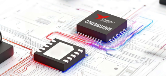
Corebai CBM12AD1X series (including CBM12AD11 single-channel and CBM12AD12 dual-channel) high-integration weak signal acquisition ASIC chips leverage the proprietary CBM ADC™ charge balancing modulation technology. By integrating complex analog front-ends into a single chip, they enable the construction of the shortest pure signal chain between "sensor and digital domain" without requiring additional PGA modules. This ASIC technology precisely resolves the "impossible triangle" challenge between performance, power consumption, and cost in traditional solutions. The core breakthrough lies in directly converting μV-level analog signals to digital signals through charge balancing modulation principles, bypassing the lengthy "amplification-filter-conversion" chain in conventional approaches. This fundamentally addresses the core conflicts of noise, power consumption, and size, providing integrated solutions with "high performance + low power consumption + high cost-effectiveness" for scenarios like thermopile detection and low-side current sensing. The solution helps customers shorten R&D cycles and accelerate product market entry.
l The core architecture utilizes CBM ADC™'s direct-to-digital conversion technology for micro-signal processing, eliminating the need for PGA and complex multi-stage amplification chains to achieve the shortest signal path. The single-chip design integrates two main ADCs (ADC0 and ADC1), two FIFO buffers (ADC0 FIFO and ADC1 FIFO), and a temperature-sensing ADC, with a system clock supporting 32kHz or 256kHz at 8x oversampling.
l Key specifications: Output LSB of 2.5μV, SNR of 84dB, 60dB suppression of second harmonic and 70dB suppression of third harmonic; ADC effective number of bits (ENOB) 14-bit, full-scale input voltage ±82mV (differential); Common-mode rejection ratio (CMRR) 110dB at 0V input and 91dB at 40mV input; Power supply rejection ratio (PSRR) 120dB at 0V input and 81dB at 38mV input.
l The core features include ADC offset correction (via the OFFSET_ADCx[15:0] register) and digital gain adjustment (GAIN_ADCx[7:0] register, with a range of 1-128/1024 to 1 + 127/1024), with the chip pre-calibrated for offset correction at factory.
l The integrated module combines the analog front-end (including Sigma-Delta Modulator SDM and CIC digital filter), ADC core, FIFO buffer, communication interface, and interrupt controller into a single chip, replacing 15-20 discrete components in traditional solutions.
l The interface configuration includes: an I2C communication interface (supporting up to 1000Kbps with ADDR slave address selection) and a DOCI single-line transmission interface. The SDA pin can be reused as an interrupt output, supporting both conversion completion and conditional interrupts to reduce the master controller's duty cycle. It also features GPIO0 and GPIO1 pins for user interface input/output operations.
l Channel control: CBM12AD11 (single channel) defaults to ADC0 only, with ADC1 disabled via ADC1_DIS register; CBM12AD12 (dual channel) defaults to both ADC0 and ADC1 enabled, supporting independent control of their switch states through ADC0_DIS and ADC1_DIS registers.
l Sampling rate configuration: Supports high-performance modes from 125Hz to 1kHz and up to 8kHz high-speed mode. By combining CLK_DIV[1:0] (SDM clock divider ratio) and SP_RATE[1:0] (sampling rate reduction), it enables multiple data rates including 125Hz, 250Hz, 500Hz, 1kHz, 2kHz, 4kHz, and 8kHz.
l Filtering capability: Equipped with a built-in CIC extraction filter, combined with a programmable low-pass filter (cut-off frequency 1Hz~4kHz) and a programmable high-pass filter (cut-off frequency 0.1Hz~100Hz), eliminating the need for external filter circuits. The channel isolation reaches 120dB, effectively preventing multi-channel crosstalk.
l Impedance characteristics: The adjustable range of input impedance is 10GΩ~1.28TΩ, and the equivalent differential input capacitance is less than 1.5pF, which can effectively reduce the signal attenuation and high frequency loss of high resistance sensors.
l Power consumption: The standby mode current drops to 2μA. At 1kpps sampling rate, the single-channel continuous operating current is 40μA and 60μA for dual-channel operation. At 500sps sampling rate, the single-channel current is 30μA and 40μA for dual-channel operation. The 1kpps window sampling mode consumes only 9μA. The operating voltage spans a wide 2.2V~3.6V range, compatible with both lithium batteries and linear power supplies.
l Packaging options: The DFN-8 package (2mm×2mm, 0.5mm pin pitch) is compatible with standard SMT surface-mount technology. Bare die (945μm×1390μm) with 60×60μm pads is also available.
l Environmental resistance: Operating temperature range-40 to 85°C, storage temperature-45 to 125°C, compliant with industrial-grade standards. Static discharge (HBM): 1000V for ADC input pins, 4000V for other IO pins. Static discharge (CDM): All pins withstand 500V. Meets RoHS standards with MSL3 humidity sensitivity rating.
l Pin protection: ADC input voltage range-0.6~0.6V (common mode to VSS), power supply voltage range-0.3~3.6V (VDD to VSS), digital input voltage range 0~VDD (GPIO0/GPIO1).
l I2C features: Bus load support 30pF, external pull-up resistor ≥800Ω, compatible with mainstream MCUs (STM32, PIC, etc.).
l DOCI interface parameters: Schmitt trigger voltage (low to high 2.0V, high to low 1.3V(VDD=3.3V); pull-down current 41.1μA, pull-up current 40.7μA, input capacitance 5pF; data clock duration ≥3μs (both low/high), data bit stabilization time ≥1μs, serial interface interrupt time 128-1024 ADC sampling clock.
l Digital IO Performance: GPIO0/GPIO1 features built-in pull-up resistors (39-109KΩ) with Schmitt trigger thresholds of 2.0V (low-to-high) and 1.3V (high-to-low). The digital output maintains a low level ≤0.4V and a high level ≥2.4V(VDD=3.3V, delivering maximum current of 28.1mA for low-level outputs and 18.6mA for high-level outputs.
Thermopile detector: Adapted to the weak signal output of thermopile sensor, single chip design simplifies the layout of the product, and low power consumption characteristics support long battery life of portable devices.
Low-side current detection: Low power consumption and wide input range are suitable for micro current monitoring scenarios. The I2C interface can quickly connect to the main controller to simplify circuit design.
Portable precision instrument: ultra-small packaging and high integration characteristics meet the space requirements, high precision index ensures the accuracy of measurement data.
010-62106066
( Monday to Friday 9:00 - 18:00 )
 704-705, Block D, Building 2, No. 9 Fenghao East Road, Haidian District, Beijing

Wechat Public Account

This app respects and protects the privacy of all users who use the service. In order to provide you with more accurate and personalized services, this app will use and disclose your personal information in accordance with this Privacy Policy. However, this application will treat this information with a high degree of diligence and prudence. Except as otherwise provided in this Privacy Policy, this application will not disclose or provide this information to third parties without your prior permission. This app will update this privacy policy from time to time. By agreeing to this Application Services Use Agreement, you are deemed to have agreed to the entire content of this Privacy Policy. This Privacy Policy is an integral part of this Application Service Agreement.
 A/D Converters (ADC)
 RF Transceiver
 Controller
 Power Management
 Logic gates
 Real-time clocks
 Digital Isolator
 Darlington Transistor
 D/A Converters (DAC)
 Sensors
 Analog Switches Multiplexers
 Interface
 Monitoring Circuit
 Amplifier
 在线商城
在线商城