
 Released:2025-10-17 15:10:26
 Views 1400 次
 作为硬件设计工程师,在信号切换电路开发中,常面临 “机械继电器体积大、功耗高”“普通模拟开关失真严重” 的痛点。今天要解析的 CBMG601,是一款专为解决这些问题打造的 CMOS 单刀单掷(SPST)常开模拟开关,其各项性能参数均来自实测数据,从电源适配到场景落地均贴合工业级需求,下面从核心特性到实际应用展开全面说明。 一、产品定位:机械继电器的高可靠性替代方案 CBMG601 采用 CMOS 工艺,核心结构为单刀单掷(SPST),默认设计为常开(NO)模式 —— 仅需通过 TTL/

As a hardware design engineer, I frequently encounter challenges in signal switching circuit development, such as "mechanical relays 'bulky size and high power consumption" and "severe distortion in conventional analog switches." The CBMG601, which we'll analyze today, is a CMOS SPST normally open analog switch specifically engineered to address these issues. All its performance parameters are derived from real-world measurements, meeting industrial-grade requirements from power adaptation to practical implementation. Below, we'll provide a comprehensive overview from core features to real-world applications.

The CBMG601 employs CMOS technology with a single-pole single-throw (SPST) core structure, defaulting to normally open (NO) mode. It requires only TTL/CMOS-compatible logic signals (IN pin) to control switching: a '1' input activates the switch, while a '0' deactivates it. With no complex timing configuration needed, this makes it highly user-friendly.
Compared with the traditional mechanical relay, its advantages are particularly outstanding:
l Reliability is stronger: no mechanical contact wear, avoid relay failure caused by contact oxidation and aging, service life is greatly extended;
l Very low power consumption: the typical value of static current (IDD) is only 0.001μA, and the maximum value is not more than 1μA, which is far lower than the mA power consumption of mechanical relays, and is friendly to the battery power supply system;
l Compact packaging: Available in 6-pin SOT-23 and 8-pin MSOP variants, the PCB footprint is reduced by over 50% compared to standard relays, making it ideal for miniaturized device designs.
l Low distortion characteristics: the typical value of on resistance is less than 3.3Ω, and the on resistance flatness is excellent, especially suitable for signal distortion sensitive scenarios.
The analog switch's core competitiveness lies in four key dimensions: conduction performance, power adaptation, signal integrity, and environmental reliability. The CBMG601's measured parameters precisely meet industrial-grade requirements, as detailed below:
It supports dual power supply mode (±2.7V to ±5.5V) and single power supply mode (+2.7V to +5.5V), eliminating the need for additional power conversion modules. This enables seamless integration into systems with different voltage architectures, such as industrial control systems (commonly ±5V) and portable devices (typically 3.3V), without requiring separate power type selection, significantly reducing design complexity.
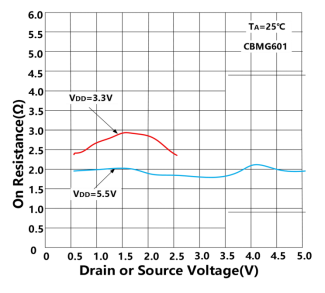
Conduction resistance and flatness are key indicators affecting signal transmission quality. The measured data are optimized according to the "double power supply" and "single power supply" scenarios to meet different design requirements.
l Dual-supply scenario (VDD=+4.5V,VSS=-4.5V, operating temperature-40℃ to +85℃): Typical on-resistance (Ron) ranges from 2Ω to 3.3Ω; typical on-resistance flatness (RFLAT(ON)) ranges from 0.2Ω to 0.75Ω. The minimal resistance fluctuation within the ±4.5V signal range effectively prevents signal distortion.
l Single power supply scenario (VDD=+4.5V, GND=0V, operating temperature-40℃ to +85℃): The typical on-resistance value is 3.5Ω, the maximum value is 8Ω, which meets the requirements of medium and high precision signal transmission, especially suitable for power sensitive single power supply system.
l Rail-to-rail operation: The input signal range covers the power rail during conduction — 0V to VDD for single power supply, and VSS to VDD for dual power supply. This eliminates signal clipping concerns, enabling direct transmission of 0~3.3V full-amplitude analog signals in 3.3V single-supply systems.
l Bidirectional conductivity: The source (S) and drain (D) pins have no fixed input/output direction, allowing bidirectional signal transmission during conduction. This enables both 'input signal switching' and 'bidirectional power path control', reducing component selection constraints.
l Wide temperature range: operating temperature range-40℃ to + 85℃, storage temperature range-65℃ to + 150℃, can operate stably in extreme high and low temperature environments (such as outdoor testing equipment, avionics equipment);
l ESD protection: With 2kV electrostatic protection capability, it reduces the risk of damage to chips caused by static electricity during production and use, and improves the system's anti-interference capability.
l Low leakage current: The maximum leakage current is ±1nA in both off and on states (consistent in dual/single power scenarios), preventing interference from weak signals (e.g., MEMS sensor signals) and ensuring data acquisition accuracy.
CBMG601 offers two miniaturized packages with identical electrical performance, with selection based solely on PCB space and soldering process considerations.

Both models are packaged in "tape and reel" with 3000 units per reel, suitable for automated mounting production lines and mass production requirements.
The pin configuration of CBMG601 is straightforward and well-defined. While both MSOP-8 (8-pin) and SOT23-6 (6-pin) packages share identical core functions, the MSOP-8 variant features two additional NC pins. The specific definitions and design considerations are as follows:

Based on actual performance, the CBMG601 demonstrates outstanding performance in the following scenarios and can be directly deployed:
1. Automatic Test Equipment (ATE): Low on-resistance flatness (maximum 0.75Ω) ensures low distortion of test signals, 180MHz bandwidth (dual power scenario) meets medium and high frequency test requirements, and effectively improves test accuracy;
2. Battery power system: 1μA static current greatly extends battery life, such as portable sensor module, a single lithium battery power can achieve several months of standby;
3. Communication system and data acquisition: The rail-to-rail signal range covers the full amplitude of the communication signal, and the ±1nA leakage current reduces the acquisition error, suitable for 4G/5G base station signal switching or industrial sensor data acquisition;
4. Power distribution: Bidirectional conductivity enables multi-path power switching. For example, in redundant power systems, the CBMG601 facilitates seamless switching between primary and backup power sources while maintaining low power consumption to minimize energy waste.
5. Avionics: Industrial-grade wide temperature range (-40℃ to +85℃) with ESD protection (2kV), suitable for harsh working environment in aviation field.
In practical design, it is essential to strictly adhere to the measured parameter boundaries specified in CBMG601 to prevent component damage.
6. Voltage limits: The maximum voltage difference between VDD and VSS is 13V, VDD to GND voltage range is-0.3V to +6.5V, analog/digital input voltage range is-0.3V to VDD+0.3V. Exceeding these limits will cause permanent damage to the chip.
7. Current Limitations: The maximum continuous current for S/D pins is 100mA, and for pulse current (1ms pulse with duty cycle ≤10%) is 200mA. It is recommended to incorporate an external overcurrent protection circuit (e.g., a series self-resetting fuse).
8. Welding temperature control: the pin welding temperature should not exceed 300℃ within 10 seconds, and the infrared reflow temperature should not exceed 260℃ to avoid high temperature damage to the internal structure of the chip;
9. Power supply filtering: A 0.1μF ceramic capacitor is connected in parallel between VDD, VSS and GND to reduce power supply noise interference to the analog signal and improve signal stability.
Summary: Clear adaptation and limitations, more accurate selection
CBMG601 is a cost-effective solution for industrial-grade medium-to-high precision analog switching applications. It overcomes the size and power consumption limitations of mechanical relays while avoiding the distortion issues of conventional analog switches. This makes it ideal for scenarios requiring current ≤100mA, frequency ≤180MHz, and stringent demands for reliability and miniaturization.
010-62106066
( Monday to Friday 9:00 - 18:00 )
 704-705, Block D, Building 2, No. 9 Fenghao East Road, Haidian District, Beijing

Wechat Public Account

This app respects and protects the privacy of all users who use the service. In order to provide you with more accurate and personalized services, this app will use and disclose your personal information in accordance with this Privacy Policy. However, this application will treat this information with a high degree of diligence and prudence. Except as otherwise provided in this Privacy Policy, this application will not disclose or provide this information to third parties without your prior permission. This app will update this privacy policy from time to time. By agreeing to this Application Services Use Agreement, you are deemed to have agreed to the entire content of this Privacy Policy. This Privacy Policy is an integral part of this Application Service Agreement.
 A/D Converters (ADC)
 RF Transceiver
 Controller
 Power Management
 Logic gates
 Real-time clocks
 Digital Isolator
 Darlington Transistor
 D/A Converters (DAC)
 Sensors
 Analog Switches Multiplexers
 Interface
 Monitoring Circuit
 Amplifier
 在线商城
在线商城