
 Released:2025-09-30 10:56:20
 Views 1256 次
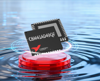
 在高速信号采集领域,模数转换器(ADC)是模拟信号与数字信号转换的‘咽喉要道’,其性能直接决定通信、雷达、卫星等系统的整体表现。芯佰微电子推出的 CBM41AD49QF 作为一款 14 位 250MSPS 高速高精度 ADC,凭借‘高动态性能 + 超低功耗 + 国产替代兼容性’三大核心优势,成为破解当前高频信号采集痛点的关键方案。该产品采用先进 CMOS 工艺制造,已实现量产,且与 TI ADS4149 引脚兼容,为设备厂商提供了高性能与供应链安全兼具的优选方案。 行业需求升级与传统方案的深

In high-speed signal acquisition, the analog-to-digital converter (ADC) serves as the critical interface between analog and digital signals, with its performance directly determining the overall performance of systems such as communications, radar, and satellite technology. CBM41AD49QF, a 14-bit 250MSPS ADC developed by Corebai Microelectronics, addresses current challenges in high-frequency signal acquisition through three core advantages: high dynamic range, ultra-low power consumption, and compatibility with domestic alternatives. Manufactured using advanced CMOS technology and already in mass production, this product maintains pin compatibility with TI ADS4149, offering equipment manufacturers an optimal solution that combines high performance with supply chain security.
With the rapid development of 5G communication, phased array radar, low-orbit satellite and other fields, signal acquisition system has put forward more stringent requirements on ADC performance, but the traditional scheme has three difficult contradictions.
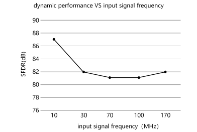
The inherent conflict between dynamic performance and operating frequency becomes particularly pronounced. In radar systems and broadband communication scenarios, when input signal frequencies exceed 170MHz, the spurious-free dynamic range (SFDR) of conventional ADCs significantly degrades, typically dropping below 70dB. This degradation causes strong signal spurious components to overwhelm weak target signals. Modern communication systems, however, require ADCs to simultaneously process multiple carrier signals while maintaining high spurious suppression across wide frequency ranges—a capability that traditional solutions can no longer meet.
The balance between power consumption and performance is equally tricky. To cover broadband signals, ADC needs to support sampling rates above 250MSPS, but the traditional solution generally consumes more than 450mW, which can lead to serious heat and a sharp drop in battery life in energy-constrained devices such as satellites and drones.
With the rapid growth of China's ADC chip market, the contradiction between supply chain security and design costs has become increasingly prominent. Mainstream imported ADC products face delivery cycles of up to 12 weeks, while domestic alternative products often require redesigning circuit boards due to differences in pin definitions and timing logic. This not only extends the R&D cycle by 3-6 months but also increases design costs by over 20%. This dilemma of "replacement means reconstruction" leaves equipment manufacturers struggling to choose between supply chain security and R&D efficiency.
CBM41AD49QF comprehensively solves the pain points of traditional solutions through four core technological innovations, and redefines the performance standards of medium and high-end high-speed ADC.

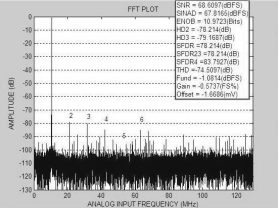
The product's most prominent advantage lies in its high-frequency dynamic performance. At a 250MHz sampling rate, when the input signal frequency is 30MHz, it achieves a Signal-to-Noise Ratio (SNR) of 70dBFS and an Uncluttered Dynamic Range (SFDR) of up to 82dBFS. Even when the input frequency increases to 170MHz, the SNR remains at 69dBFS and SFDR stays above 76dBFS. This exceptional high-frequency capability stems from the collaborative design of a multi-stage pipeline architecture and digital correction circuits, ensuring effective noise and spurious signal suppression across a wide frequency range to meet the demands of multi-carrier communication and radar weak signal detection. Additionally, the 14-bit resolution combined with-0.99~+0.8LSB differential nonlinearities (DNL) and ±3.5LSB typical integral nonlinearities (INL) achieves precise quantization without bit loss.
The ultra-low power design challenges the industry's conventional belief that "high performance requires high power consumption." The CBM41AD49QF operates on a single 1.8V supply, achieving simulated power consumption of 248.4-270mW in LVDS mode and 117-144mW in digital mode. Through optimized design and reduced supply voltage, it achieves over 30% lower total power consumption compared to traditional solutions. Notably, its flexible power management mechanism reduces power consumption to 3.5-25mW during sleep mode, making it particularly suitable for energy management in intermittent operation scenarios like satellite systems. This power advantage stems from CMOS process optimization and innovative circuit architecture, achieving a significant leap in energy efficiency while maintaining high performance.
The highly flexible configuration capability significantly enhances scenario adaptability. Through the SPI interface, users can precisely configure internal registers: For LVDS output swing, it supports an adjustable range from ±125mV to ±570mV. Selecting high swing enhances anti-interference capability during long-distance transmission, while low swing reduces EMI during short-distance transmission. Gain adjustment supports 0-6dB stepwise adjustment. In multi-carrier scenarios, increasing the gain by 3dB can optimize SFDR by 2-3dB. Additionally, data format supports two-complement/offset binary switching, with interface modes compatible with LVDS/DDR LVDS/CMOS, meeting the adaptation requirements of different backend processing chips.
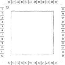
The domestically developed PIN-compatible alternative solution ensures supply chain security. This product is fully pin-compatible with TI ADS4149, enabling direct replacement without PCB design modifications, which significantly reduces replacement costs and R&D risks. Its QFN-48 package design not only features a compact size but also optimizes thermal performance through exposed pads. Combined with independent Grounding for Analog (GNDA) and Digital (GNDD) designs, it effectively suppresses digital noise interference on analog signals, thereby simplifying high-speed PCB layout.
In wireless broadband communications, the combination of 250MSPS sampling rate and 480MHz analog input bandwidth meets the real-time acquisition requirements for wideband signals in 5G base station receivers. The 82dBFS with high SFDR effectively suppresses intercarrier interference and enhances multi-carrier signal demodulation quality, making it particularly suitable for complex communication environments in densely populated urban areas.
Operating at 170MHz high-frequency input, this product maintains a 76dBFS spurious-free dynamic range (SFDR), ensuring precise differentiation of strong and weak target signals in radar echoes. With an exceptional wide operating temperature range spanning-40℃ to 85℃ and a mere 3.5mW sleep power consumption, it stands as the ideal choice for satellite payloads, delivering robust performance in extreme environments while meeting stringent energy constraints.
In the field of communication testing equipment, 14-bit high resolution with 10.5Bit effective bits (ENOB) ensures measurement accuracy for signal analyzers and spectrum analyzers. The parallel interface features a data setup time ≥0.35ns and hold time ≥0.75ns, meeting the stringent timing requirements of real-time data processing. For power amplifier (PA) monitoring, its high linearity characteristics enable precise detection of output signal distortion, providing accurate data support for linearization adjustments.
010-62106066
( Monday to Friday 9:00 - 18:00 )
 704-705, Block D, Building 2, No. 9 Fenghao East Road, Haidian District, Beijing

Wechat Public Account

This app respects and protects the privacy of all users who use the service. In order to provide you with more accurate and personalized services, this app will use and disclose your personal information in accordance with this Privacy Policy. However, this application will treat this information with a high degree of diligence and prudence. Except as otherwise provided in this Privacy Policy, this application will not disclose or provide this information to third parties without your prior permission. This app will update this privacy policy from time to time. By agreeing to this Application Services Use Agreement, you are deemed to have agreed to the entire content of this Privacy Policy. This Privacy Policy is an integral part of this Application Service Agreement.
 A/D Converters (ADC)
 RF Transceiver
 Controller
 Power Management
 Logic gates
 Real-time clocks
 Digital Isolator
 Darlington Transistor
 D/A Converters (DAC)
 Sensors
 Analog Switches Multiplexers
 Interface
 Monitoring Circuit
 Amplifier
 在线商城
在线商城