 Released:2025-08-29 10:36:09
 Views 1386 次
 总述: 光模块作为光通信系统的‘微观核心’,其性能直接决定了网络带宽、传输距离与能源效率。从数据中心的‘算力动脉’到电信网络的‘信息干线’,再到工业与车载领域的‘智能神经’,光模块已深度融入数字社会的每一层架构。在AI与6G时代海量数据需求的驱动下,光模块技术正以前所未有的速度演进,不断拓展光互联的边界。

Summary:
As the "micro-core" of optical communication systems, optical modules directly determine network bandwidth, transmission distance, and energy efficiency. From serving as the "computing power arteries" in data centers to acting as the "information backbone" in telecom networks, and further functioning as the "intelligent nervous system" in industrial and automotive applications, optical modules have become deeply integrated into every layer of digital society's architecture. Driven by the massive data demands of the AI and 6G eras, optical module technology is evolving at an unprecedented pace, continuously expanding the boundaries of optical interconnection.

Current optical module design and application still face a number of key technical challenges:
l DAC precision: DAC needs high precision conversion MCU digital instructions to drive EML/DFB laser for accurate dimming;
l Poor universality of driver circuit: EML/DFB Driver needs to accurately match the laser threshold current, modulation efficiency and other characteristics. Different wavelength/power devices have strict requirements on linearity and response speed, and there is no widely applicable driver scheme.
l Simulated link noise suppression problem: Limited Amplifier needs to maintain gain stability in complex noise environment, and coordinate with DAC and driver. Electromagnetic interference and power supply noise are easy to cause signal deterioration.
l Inadequate temperature control response rate: TEC needs to quickly compensate for the influence of temperature on laser wavelength/power. Under extreme temperature changes (e.g., -40℃~85℃), the temperature control algorithm and hardware response lag are easy to cause optical signal fluctuation, affecting the stability of long-distance transmission.
In view of the core difficulties in precision, drive, noise and temperature control of optical modules, Corebai Micro has launched an integrated chip solution covering digital-to-analog conversion, drive control, signal conditioning and temperature management to provide key support for customers to build high-speed, stable and reliable optical communication systems.

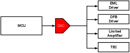
Light module application block diagram
The Corebaiwei DAC chip delivers high-precision digital-to-analog conversion, accurately transforming MCU digital commands into analog signals. It provides stable drive voltage/current for EML and DFB drivers while precisely controlling laser power and wavelength. With its high bandwidth characteristics, the chip meets the signal requirements of high-speed optical modules, ensuring distortion-free signal conversion and enabling optical modules to achieve efficient, stable light signal transmission.


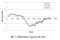
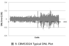
l High-precision conversion: 12-bit resolution with INL ±2LSB and DNL ±0.2LSB, delivering accurate analog output. The output voltage ranges from 0V to VREF, featuring an integrated rail-to-rail buffer amplifier and a DC output impedance of just 0.5Ω. It reliably drives 2kΩ loads and 500pF capacitive loads, with short-circuit current reaching 25mA at 5V.
l Wide temperature working capacity: the operating temperature range is-40℃~105℃, the gain error is ±0.75% FSR at 85℃, with good temperature stability, suitable for all kinds of harsh industrial environment.
l Ultra-low power design: standard mode current is 500μA when powered by 3V,600μA when powered by 5V; sleep mode current is low to 80nA@3V,200nA@5V, very suitable for battery powered or strict power consumption requirements applications.
l Flexible interface and synchronous control: The 3-line SPI compatible interface supports binary complement/offset code output with a maximum clock frequency of 30MHz. Through dual buffer logic, the LDAC bit control register can be updated to achieve four-way output synchronization refresh, avoiding timing deviation.
l Wide power supply voltage range: the power supply voltage range is 2.5V to 5.5V, the common mode rejection ratio of the power supply is-60dB, can effectively suppress the impact of ±10% power supply fluctuation on the output precision, suitable for the complex power supply environment in industrial scenarios.
l Reference voltage input optimization: The reference input voltage range is 0.25V~VDD, and the typical impedance is 45kΩ. In order to maintain the best reference stability in a wide temperature environment, it is recommended to use an external buffer.
l High resolution: With 12-bit resolution, it can provide high analog output accuracy and can be used in applications requiring high precision, such as industrial control, data acquisition and other fields.
l Multiple channel output: The single chip integrates 8-channel voltage output analog-to-digital converter with output buffer driver, which can meet the needs of multiple analog signals in various application scenarios.
l Wide voltage range: The normal operating power supply voltage range is 2.7V~5.5V, which can adapt to a variety of different power conditions, reducing the requirements for the power supply and improving the applicability of the chip. Its I/O voltage is 1.8V~5.5V, and the Core voltage is 1.8V~3.6V.
l Low power consumption: When not in use, the total current consumption is only 540μA@3V or 600μA@5V. When all digital-to-analog converters enter sleep mode, the chip operates at μW level power consumption, making it ideal for portable devices or applications with strict power requirements.
l High-speed interface: adopts three-line serial interface, the maximum clock can reach 40MHz, allows very flexible configuration, compatible with the current common SPI, QSPI, MICROWIRE and DSP interface standards, support chrysanthemum chain mode of work, can use a single interface to control multiple chips at the same time, ensure that multiple chips are updated at the same time.
l High precision characteristics: The integral nonlinearity (INL) is ±2 LSB, and the differential nonlinearity (DNL) ensures monotonicity at ±0.2 LSB. The zero code error temperature drift is-20μV/℃, and the gain error temperature drift is-1.0 ppm/℃. It provides highly accurate analog output, meeting the requirements of high-precision applications.
l Flexible reference voltage configuration: Featuring two external reference voltage inputs, one dedicated to Channels A-D and the other for Channels E-H. Each reference voltage supports individual configuration with a wide input range from 0.5V to VDD, enabling the chip to deliver versatile dynamic signals that meet diverse application requirements.
With high-precision DAC and other chip technologies, Corebaiwei enables optical modules to adapt to multiple scenarios and give full play to the value of signal precision control:
Scenario: Industrial automation production line (such as automobile manufacturing, electronic processing), intelligent factory park interconnection, need to deal with high temperature, vibration, electromagnetic interference complex environment.
Scheme value: Corebai Micro DAC and driver circuit work together to ensure the stability of optical signals in industrial SFP optical modules within the wide temperature range of-40℃~85℃, provide reliable optical links for PLC control and machine vision, and support intelligent production line and high reliability operation.
Scenario: Intelligent vehicle ADAS system, on-board Ethernet (such as in-car camera-domain controller connection), need small, anti-interference optical module.
Program value: Through high-precision DAC to achieve TEC accurate temperature control and laser stable drive, ensure that the on-board optical module can still achieve high-speed and low-latency data transmission under harsh conditions such as vibration and high temperature, and help the safe and stable operation of the autonomous driving system.
010-62106066
( Monday to Friday 9:00 - 18:00 )
 704-705, Block D, Building 2, No. 9 Fenghao East Road, Haidian District, Beijing

Wechat Public Account