

 Released:2026-10-27 10:03:56
 Views 28 次
 工业现场的读码设备,要把条形码上那束微弱、随扫描明暗变化的反射光,变成稳定可译码的信号并传出去——光路、放大、供电、上传,每一环都可能拖慢整机。

In industrial environments, barcode reading devices must convert the faint reflected light—whose intensity varies with the illumination during scanning—from the barcode into a stable, decodable signal, then transmit it; each stage—optical path, amplification, power supply, and data upload—can potentially slow down the overall system performance.
In this circuit design, Corebai has implemented a solution comprising three key components—the operational amplifier, the power supply, and the communication interface—utilizing the CBM8622 (dual-channel) operational amplifier to perform secondary amplification of optoelectronic signals, the CBM1117 for voltage regulation of the power supply, and the CBM9002A to handle the USB uplink functionality—converting the nA-level current output from the photodiode into decoded data for transmission via the USB port. The photodiode is a externally sourced component; the models of the ADC, LED driver, and main control MCU are determined based on the overall system design.

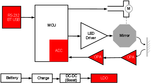
This solution employs the main control MCU as its core control unit and comprises four coordinated communication links:
Optical path drive chain: MCU → LED driver → LED → mirror → barcode
Signal acquisition chain: reflected light → photodetector → two-stage amplification → ADC → MCU
Power supply chain: Battery → Charging circuit → DC-DC Boost → CBM1117 LDO
Communication chain: CBM9002A provides a USB uplink interface → external device
During PCB layout, the analog front-end can be appropriately separated from the digital and power regions to minimize mutual interference. For photodetectors and preamplifier regions, shielding measures may be implemented based on specific requirements to mitigate the effects of ambient light and electromagnetic interference.
For LED lighting, it is recommended that the MCU output PWM control to a constant-current driver to ensure consistent illumination brightness—since the intensity of reflected light directly determines the signal amplitude, any brightness fluctuations will be amplified through both stages, thereby compromising decoding stability.
The light emitted by the LED is projected onto the surface of the barcode via a reflector; the black and white stripes of the barcode cause variations in the intensity of the reflected light, which is then converted into an electrical signal by a photodiode. The dark current and junction capacitance of the photodiode directly influence the noise floor and bandwidth of the preamplifier; ambient light, under weak signal conditions, acts as both a DC offset and a noise source, necessitating suppression through optical shielding and localized baffle design; furthermore, the LED driver should incorporate a dimming interface.
The current signal output from a photodiode has a very small amplitude and is susceptible to noise; therefore, a two-stage architecture consisting of "transimpedance amplification followed by voltage amplification" is commonly employed before feeding the signal to the ADC. These two stages can be implemented using the CBM862X series of operational amplifiers from Corebai—specifically the CBM8621, CBM8622, and CBM8624, which represent single-, dual-, and quad-op amp variants of this series, respectively; models bearing the "S" suffix feature a shutdown function. This series is suitable for photodiode signal amplification and sensor interfacing, making it compatible with code-reading front-ends.
The key parameters of this series include: a 7 MHz gain-bandwidth product, a slew rate of 3.7 V/μs, and a typical input offset voltage of 0.7 mV; it supports single-supply or dual-supply operation, with a single-supply range of 2.5–5.5 V and a dual-supply range of ±1.25–±2.75 V; at Vs = 5.5 V, the minimum input voltage range is −0.1 V; the operating temperature range is −40–125 °C, it supports rail-to-rail input and output, and can operate stably at unity gain.
First stage (transimpedance preamplification): The feedback resistor converts the photocurrent from the photodiode into a voltage. Increasing the feedback resistor value can enhance the conversion gain, but it may also adversely affect bandwidth and noise; the appropriate value should be determined based on the response characteristics and junction capacitance of the photodiode.
Stage 2 (Filtering and ADC Driving): A non-inverting amplifier can be employed, with an RC network used to suppress out-of-band noise, thereby conditioning the signal to fit within the input range of the ADC. A slew rate of 3.7 V/μs and a typical input offset voltage of 0.7 mV provide the foundation for linear amplification; whether these parameters satisfy the linearity requirements for medium-to-high-speed decoding must be verified through integrated analysis of photodiode characteristics, the feedback network, and the ADC input range design.
The CBM8622 is a dual-op-amp model; selecting a single unit suffices to cover the two amplification stages mentioned above. If the system also requires level conversion or buffering, it is advisable to evaluate the use of the CBM8624, which offers more channels; if fewer channels are required, the CBM8621 can be selected instead. Cascading these two stages can amplify weak photoelectric signals to values close to the ADC input range; the final gain allocation and ADC range utilization should be determined based on the specific circuit design. When combined with appropriate filtering, power supply, and grounding layouts, this configuration can suppress out-of-band interference and power-supply coupling noise according to design objectives; however, the actual noise performance will still depend on the external circuitry and PCB layout.
The analog signal is sampled by the ADC and then fed into the MCU, which performs barcode decoding. The power supply for the ADC can be provided by the CBM1117 power chain; the allocation, decoupling, and grounding of analog and digital power supplies should be integrated with the design of the selected ADC to minimize noise coupling; the ADC reference source must be designed separately, with verification based on the specific model. The MCU can employ an adaptive threshold algorithm to interpret black-and-white stripes, offering improved fault tolerance under low-light and high-reflectivity conditions; the performance of this algorithm should be validated under actual lighting conditions, material properties, and scanning environments.
Handheld devices can be powered by batteries, the voltage of which varies with the battery state of charge. After being charged via a charging circuit, the battery can be stepped up by a DC-DC boost converter, followed by linear regulation via the CBM1117; the battery type and boost voltage should be determined based on the overall power consumption of the device and the requirements of its power rails.
The CBM1117 series delivers an output current of up to 0.8 A, featuring fixed-output versions at 1.5 V, 1.8 V, 2.5 V, 3.3 V, and 5.0 V, as well as an adjustable (ADJ) version. It supports a maximum input voltage of 15 V, offers a load regulation rate of up to 0.4% (typical: 0.2%), incorporates built-in current limiting and overtemperature protection, and operates within a temperature range of −40–125 °C. Available in SOT-223 and TO-252 packages, this series provides regulated power supplies for MCUs, photodetectors, and operational amplifiers; actual noise suppression performance depends on the power supply design and PCB layout.
The available power rail depends on the Boost output voltage and the selected CBM1117 model: for a 5 V bus, the fixed 3.3 V version has an input range of 4.75–10 V, enabling direct power supply to the MCU and digital sections; if the analog front-end or LED driver requires a 5 V power rail, the 5.0 V output version has an input range of 6.5–12 V, in which case the Boost voltage should be increased accordingly, or the ADJ version should be selected with the voltage set according to the actual voltage difference.
Placing a 10 μF tantalum capacitor at the LDO output terminal can enhance transient response and stability; implementing separate routing for analog and digital power supplies, along with placing decoupling capacitors in close proximity to the devices, helps reduce interference in sampled signals; additionally, shortening feedback traces near the photodetector and the first-stage operational amplifier, and implementing appropriate grounding and shielding measures based on specific conditions, can further suppress ambient light and RF interference.
The main control MCU is responsible for sampling control and barcode decoding, and can also control the LED driver and the scanning motor based on the system design; the motor control method, the mirror rotation speed, and the scanning range shall be determined in accordance with the optical-mechanical structure. The decoding results are uploaded via a USB interface or, optionally, an RS-232 interface.
The CBM9002A is a microcontroller integrating an enhanced 8051 core and a USB interface, capable of performing the functions of a USB microcontroller. Its core operating frequencies support 48 MHz, 24 MHz, and 12 MHz (with instruction throughput approximately three times that of a standard 8051), it features 16 KB of on-chip SRAM, and integrates interfaces such as UART, I2C, and GPIO. The industrial-grade variant operates within a temperature range of −40 °C to 105 °C, and is available in SSOP56, QFN56, and LQFP100 packages.
The CBM9002A supports both USB 2.0 high-speed mode and full-speed mode; within a specified firmware framework, it can achieve a data transmission rate exceeding 50 MB/s via the Slave FIFO/PIF interface—this figure represents the interface transmission capability, while the actual barcode scanning data rate of the complete device is determined by the implementation of the firmware and the host system. This solution provides a USB uplink interface for uploading barcode scanning data; the firmware can be downloaded via USB or loaded from an external EEPROM. The specific division of responsibilities between the CBM9002A and the main control MCU shall be determined based on the overall system design.
If you need to connect to an industrial PLC or other legacy terminals featuring an RS-232 interface, the CBM3232 can be used as an optional transceiver (separate from the main signal chain). The CBM3232 comprises two receivers and one driver, guaranteeing a maximum data rate of 120 Kbps; this interface also supports USB integration, enabling compatibility with both legacy and modern device interfaces, with the specific choice depending on the requirements of the end device.
|
Signal chain position |
Recommended Models |
key parameter |
remarks |
|
Photoelectric reception |
photodiode |
Low dark current, small junction capacitance |
The preamplification input should be shielded. |
|
Two-stage amplification (transimpedance + drive) |
CBM8622 (Dual-channel, 862X series) |
7 MHz GBW, 3.7 V/μs, 0.7 mV offset, rail-to-rail, 2.5–5.5 V, −40–125 °C |
One model covers two levels; in terms of margin, CBM8624 (four-channel) |
|
Power Voltage Regulation |
CBM1117 |
0.8 A, fixed/adjustable, maximum load adjustment 0.4% (typical: 0.2%), −40–125 °C |
LDO secondary voltage regulator, regulated output |
|
USBcommunication |
CBM9002A |
USB 2.0: high-speed 480 Mbps / full-speed 12 Mbps; industrial-grade temperature range: −40–105 °C |
USB microcontroller with USB uplink; industrial wide-temperature range |
|
(Optional) RS-232 extension |
CBM3232 |
RS-232 transceiver (2 receive, 1 drive; guaranteed maximum speed of 120 Kbps), compatible with PLCs and legacy terminals |
Complements USB, supporting PLCs and legacy terminals. |
|
(Optional) DC-DC Boost |
— |
Step up the battery voltage to the required bus voltage (e.g., 5 V, as specified in the CBM1117 output configuration). |
Compatible with CBM1117 |
The actual barcode reading performance depends on the optical structure, photoelectric detection, amplification and sampling, decoding algorithms, and PCB design. During implementation, one can first verify the output range of the photodiode and the input range of the ADC, then determine the amplification and filtering parameters, and finally validate the overall system performance using the target barcode and the specified scanning conditions.
010-62106066
( Monday to Friday 9:00 - 18:00 )
 704-705, Block D, Building 2, No. 9 Fenghao East Road, Haidian District, Beijing

Wechat Public Account


This app respects and protects the privacy of all users who use the service. In order to provide you with more accurate and personalized services, this app will use and disclose your personal information in accordance with this Privacy Policy. However, this application will treat this information with a high degree of diligence and prudence. Except as otherwise provided in this Privacy Policy, this application will not disclose or provide this information to third parties without your prior permission. This app will update this privacy policy from time to time. By agreeing to this Application Services Use Agreement, you are deemed to have agreed to the entire content of this Privacy Policy. This Privacy Policy is an integral part of this Application Service Agreement.


 Online Store
 A/D Converters (ADC)
 RF Transceiver
 Controller
 Power Management
 Logic gates
 Real-time clocks
 Digital Isolator
 Darlington Transistor
 D/A Converters (DAC)
 Sensors
 Analog Switches Multiplexers
 Interface
 Monitoring Circuit
 Amplifier


 在线商城
