

 Released:2026-09-01 13:27:09
 Views 402 次
 ▶ 8 通道 12 位电阻串 DAC,INL ±2 LSB、DNL ±0.2 LSB 保证单调性 ▶ 空载功耗 540µA@3V、休眠典型 10µA,全休眠后 µW 级功耗 ▶ 三线 SPI 40MHz + 菊花链,多芯片同一时刻同步更新 ▶ 上电/断电双复位,−40~125℃ 工业宽温

[Key Highlights – Preview]
▶ 8-channel, 12-bit resistor-string DAC; INL ±2 LSB, DNL ±0.2 LSB – ensures monotonicity
▶ No-load power consumption: 540 µA @ 3 V; Typical sleep mode: 10 µA; Full sleep mode: µW-level power consumption
▶ Three-channel SPI (40 MHz) + Chrysanthemum Chain – enables simultaneous synchronous updating of multiple chips
▶ Dual power-on/off reset function; industrial wide-temperature range: −40°C to 125°C
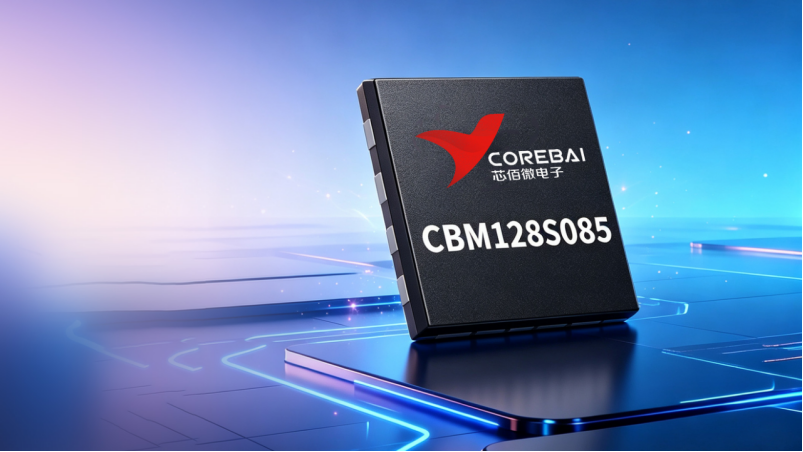
Part 1 · The Foundation of This DAC
Q1. What type of DAC is the CBM128S085, and how many channels and bits does it have?
This is an 8-channel, 12-bit voltage-output DAC with output buffer driving capability, featuring a resistor-series architecture and available in TSSOP-16 or QFN-16 package types. The normal operating supply voltage range is 2.7 V–5.5 V, and the operating temperature range is −40°C–125°C.
Selection Tip: The 8-channel integrated DAC is ideal for "multi-channel programmable voltage" applications; if only 1–2 channels are required, a single-channel DAC is more cost-effective.
Q2. Does the digital interface of CBM128S085 support low-voltage MCUs?
The CBM128S085 supports a digital I/O voltage range of 1.8 V–5.5 V, making it compatible with various level-signaling system designs. Its analog supply voltage (VA) ranges from 2.7 V to 5.5 V; therefore, designers should carefully consider both the digital interface level requirements and the analog supply requirements during design.
Q3. What is the accuracy metric?
12-bit resolution; INL ±2 LSB; DNL ±0.2 LSB with guaranteed monotonicity; maximum zero-code error: +15 mV; full-scale error: −0.1% FSR; gain error: −0.2% FSR.
Selection Note: The INL definition excludes certain maximum and minimum code values (where linearity deteriorates when the output approaches 0 V or the power supply rail); in practical applications, care should be taken to account for changes in linearity when the output approaches 0 V or 0 A.
Q4. What are the output capability and load driving capability?
Output voltage range: [0, V_A]; the upper limit is limited by the reference voltage; the rail-to-rail output buffer can drive a 2 kΩ resistance load and a 1500 pF capacitor; built-in short-circuit protection with a typical current rating of 20 mA.
Selection tip: When full-range output is required, the reference voltage should be as close as possible to the supply voltage; however, the linearity near the supply rail will decrease – therefore, strike a balance based on your actual accuracy requirements.
Part II · Reference Voltage and Serial Control
Q5. How do you configure the reference voltage?
Two external reference inputs: VREF1 supplies the A–D channels, and VREF2 supplies the E–H channels; input range: 0.5 V–V_A; input impedance: 45 kΩ; each input group can be configured independently.
Selection Tip: When designing a reference voltage source, consider a 45 kΩ reference input impedance and perform local decoupling at the VREF pin; the two reference circuits can operate at different voltage levels, offering greater flexibility.
Q6. What are the key considerations for the SPI communication timing of the CBM128S085?
The CBM128S085 features a three-wire serial interface; data is written into the shift register on the falling edge of the SCLK signal. A single communication transaction consists of 16 clock cycles; the SYNC signal is used to control the validity of the data frame. When designing the MCU driver, care must be taken to ensure proper setup and hold times for the SCLK, SYNC, and DIN signals.
Q7. How do you use the serial interface?
Three-pin interface (SCLK/DIN/SYNC), with a maximum frequency of 40 MHz; compatible with SPI, QSPI, MICROWIRE, and most DSP interfaces; data is transferred in 16-bit frames: the upper 4 bits (DB[15:12]) represent mode control, while the lower 12 bits (DB[11:0]) represent data; write operations occur on the falling edge of the clock signal; programming is triggered by the rising edge of the SYNC signal.
Selection Note: If the SYNC signal rises before the 15th clock falling edge, the current sequence is considered invalid; the timing design shall be calculated according to the setup/hold time requirements.
Q8. How do I use the Chrysanthemum Chain Mode?
All chips share the SYNC and SCLK signals; the DOUT pin of one chip connects to the DIN pin of the next chip, enabling frame-by-frame data cascading; when the rising edge of the SYNC signal arrives, all chips simultaneously update their outputs.
Selection Note: For菊花链配置,DOUT is updated on the clock's falling edge and sampled by the next downstream chip; the board-level delays for SYNC/SCLK/DIN/DOUT must be accounted for; if necessary, add a delay between DIN and DOUT.
Part III · Operating Modes and Protection
Q9. What are the dual-register and update modes?
Each channel includes a data register and a DAC register: in the WRM mode, only the data register is updated; in the WTM mode, both the data register and the DAC register are updated (output is modified directly); additionally, there are three special commands: Broadcast Mode, Channel A Update, and Update Selection.
Selection Tip: When multiple output channels need to change synchronously, first write the data to each channel using the WRM command, then apply a unified update using the Broadcast/Update Selection Command to avoid per-channel abrupt changes.
Q10. How do I use the Sleep Mode?
Each channel can be independently placed into sleep mode; the sleep output offers three selectable impedance levels: high impedance, 2.5 kΩ to ground, or 100 kΩ to ground; the typical sleep current is 10 µA; when all 8 channels are in full sleep mode, the overall chip power consumption is in the µW range.
Selection Note: The power-off reset circuit continues to operate in sleep mode (approximately 10 µA); this does not constitute a complete power-off; the output impedance setting should be selected according to the load requirements.
Q11. What are power-on reset and power-off reset?
Power-up reset sets the DAC output to 0 V when the power supply reaches an effective voltage, until the first update command is received; Power-down reset is triggered when the power supply falls below approximately 2.7 V, setting the output to 0 V to prevent any non-zero output from affecting subsequent circuit operations.
Selection Tip: This feature is ideal for systems where the output must be zero at power-on; it eliminates the need for an external reset circuit.
Part IV · Power Consumption and Dynamic Performance
Q12. What is the power consumption level?
No-load overall static current: 540 µA @ 3 V, 600 µA @ 5 V; typical sleep current: 10 µA; power consumption in µW range after full sleep mode.
Selection Tip: For the battery system, focus on the no-load and sleep modes' current values; under a 3V power supply condition, the typical current is 540 µA.
Q13. What is the dynamic performance?
Output setup time: approximately 6–8.5 µs; slew rate: 1 V/µs; output bandwidth: 350 kHz; THD+N: –80 dB (100 Hz–20 kHz); output noise: 14 µV (30 kHz bandwidth).
Model Selection Note: With a response time of approximately 6 µs, this device is designed for slow-speed programmable voltage and DC setting applications; it is not suitable for high-frequency waveform output scenarios.
Part V · Selection and Implementation
Q14. Temperature, packaging, and reliability parameters?
Operating temperature range: −40°C to 125°C; the CBM128S085QS is available in QFN-16 package (2500/windings), while the CBM128S085TS is available in TSSOP-16 package (2500/windings); additional variants include TS-RL (3000/windings) and TS-REEL (4000/windings). The products support ESD protection capabilities of 5000 V for human models, 300 V for machine models, and 1000 V for charging equipment models.
Selection Tip: The QFN and TSSOP packages have the same number of pins but differ in their pad configurations; therefore, please confirm the package selection before proceeding with layout design.
Q15. For what applications is it suitable?
Portable battery-powered instruments; digital gain and offset adjustment; programmable voltage and current sources; programmable attenuators; ADC and sensor reference voltage sources; pulse generators; range detectors; clock calibration units, etc.
Selection Tip: For applications requiring multiple low-speed programmable voltage sources, use a high-speed DAC; for scenarios requiring high-speed waveform output, use a high-speed DAC.
Q16. Alternative compatibility?
|
Model suffix |
package |
explain |
|
CBM128S085-TS |
TSSOP-16 |
Suitable for manual welding and prototype verification |
|
CBM128S085-QS |
QFN-16 |
Ideal for mass production and scenarios with limited space. |
The CBM128S085 features an 8-channel, 12-bit DAC function and supports both TSSOP16 and QFN16 package options, facilitating the domestic substitution of imported products.
Selection Note: When replacing components, carefully verify the reference voltage configuration, SPI timing, and sleep mode behavior; when requesting sample parts, specify the packaging requirements.
[Model Selection Summary]
The CBM128S085 utilizes a 16-pin chip to provide 8-channel, 12-bit voltage outputs; its resistor-series architecture ensures monotonicity and ±2 LSB accuracy, while the SPI菊花链 interface enables synchronous multi-chip updates. With a no-load current of 540 µA and a full-sleep power consumption of just µW, it is ideal for battery-powered systems. When selecting this device, ensure adequate margin is reserved for both the reference voltage and the linearity requirements – making it a stable and reliable choice for portable instruments and programmable voltage sources.
010-62106066
( Monday to Friday 9:00 - 18:00 )
 704-705, Block D, Building 2, No. 9 Fenghao East Road, Haidian District, Beijing

Wechat Public Account





This app respects and protects the privacy of all users who use the service. In order to provide you with more accurate and personalized services, this app will use and disclose your personal information in accordance with this Privacy Policy. However, this application will treat this information with a high degree of diligence and prudence. Except as otherwise provided in this Privacy Policy, this application will not disclose or provide this information to third parties without your prior permission. This app will update this privacy policy from time to time. By agreeing to this Application Services Use Agreement, you are deemed to have agreed to the entire content of this Privacy Policy. This Privacy Policy is an integral part of this Application Service Agreement.


 Online Store
 A/D Converters (ADC)
 RF Transceiver
 Controller
 Power Management
 Logic gates
 Real-time clocks
 Digital Isolator
 Darlington Transistor
 D/A Converters (DAC)
 Sensors
 Analog Switches Multiplexers
 Interface
 Monitoring Circuit
 Amplifier

 在线商城
在线商城