

 Released:2026-10-12 15:31:04
 Views 6 次
 在电池供电设备和低压传感器系统中,运算放大器既要适应有限的电源电压,也要尽量减少自身功耗,并为输入和输出信号保留足够的摆幅。CBMV321 是一款单通道、低功耗、轨至轨输入/输出运算放大器,适用于传感器信号调理、低频有源滤波及便携设备中的一般模拟信号处理。

In battery-powered devices and low-voltage sensor systems, operational amplifiers must not only accommodate limited supply voltages but also minimize their own power consumption while providing sufficient headroom for both input and output signals. The CBMV321 is a single-channel, low-power, rail-to-rail input/output operational amplifier designed for sensor signal conditioning, low-frequency active filtering, and general analog signal processing in portable devices.
The CBMV321 from Corebai Micro is a single-channel, low-power, rail-to-rail input/output operational amplifier in this series, operating within a supply voltage range of 2.5 V to 5.5 V and a temperature range of −40°C to +125°C. The device is available in SOT23-5, MSOP-8, and SOIC-8 package options, making it suitable for sensor signal conditioning, low-frequency active filtering, and single-channel analog signal processing in portable devices. When designing, the appropriate package can be selected based on PCB space constraints, assembly requirements, and circuit specifications.
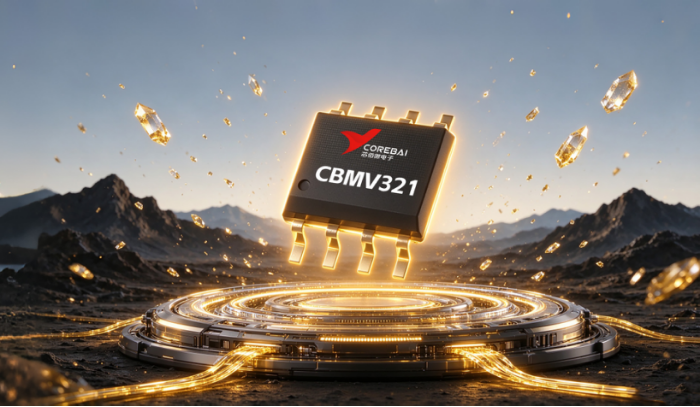
CBMV321 supports a supply voltage range from 2.5 V to 5.5 V, making it suitable for a variety of low-voltage analog circuits. This wide low-voltage supply range provides flexibility for power supply design and analog front-end integration.
In single-power-supply systems, the input signal often approaches ground potential. The common-mode input range of the CBMV321 is from −0.1 V to +5.6 V at Vs = 5.5 V, which facilitates the handling of input signals close to the power supply rail. In practical design, it is still necessary to verify that the input voltage complies with the device's rated specifications and to incorporate an appropriate margin for signal variations.
The available voltage headroom between power rails in a low-voltage system is limited. Rail-to-rail input/output characteristics help expand the input signal range and improve the utilization of the output dynamic range.
The actual output swing varies with the load. For the CBMV321, the output swing from the power rail is approximately 8 mV under a 10 kΩ load, and approximately 26 mV under a 2 kΩ load. Therefore, when operating under heavier loads or in applications where the output needs to approach the power rail, the output range should be recalculated based on the actual load, and a margin should be reserved for signal peak values.
The typical quiescent current of CBMV321 is approximately 60 μA per amplifier. For battery-powered devices, sensor nodes, and continuously operating analog front-ends, a lower quiescent current helps reduce the power consumption of the operational amplifier itself.
The actual power consumption of the system may also be affected by the supply voltage, the output load, and the peripheral circuits. The basic model of the CBMV321 does not include a shutdown function; if the design requires shutdown capability under logical control, a model featuring this functionality should be selected.
The gain-bandwidth product of CBMV321 is 1.1 MHz (typical), and its slew rate is 0.5 V/μs (typical). Both the gain-bandwidth product and the slew rate jointly determine the operational amplifier's capability to process signals of varying frequencies and amplitudes. The available bandwidth in a practical circuit may vary depending on the closed-loop gain, signal amplitude, and load conditions. For signals at higher frequencies or with larger amplitudes, it is recommended to evaluate the bandwidth and distortion performance in conjunction with the specific circuit design.
The typical input bias current of CBMV321 is 1 pA, with a maximum value of 10 pA. A lower input bias current facilitates connection to high-impedance signal sources and reduces errors caused by the bias current flowing through the signal source impedance.
The typical input offset voltage is 0.8 mV, with a maximum value of 4.5 mV. In circuits with high closed-loop gain or precision DC measurement applications, input offset may affect the system's zero-point error and should therefore be included in the error budget. Actual accuracy also depends on the feedback network, temperature variations, and the inherent errors of the sensor itself.
A lower input bias current is a design advantage; however, whether an additional buffer is required should still be determined based on the sensor's output impedance, target bandwidth, noise level, and circuit topology.
|
dimension |
parameter |
metric |
|
supply electricity |
Operating voltage range: VS |
2.5V–5.5V (single/dual power supply) |
|
Temperature class |
working temperature |
−40℃~+125℃ |
|
power dissipation |
Static current IQ (per amplifier) |
60 µA (typical) / 80 µA (maximum) |
|
accuracy |
Input offset voltage VOS |
0.8 mV (typical) / 4.5 mV (maximum) |
|
accuracy |
Average offset voltage drift VOSTC |
2.9µV/℃(−40℃~+125℃) |
|
import |
Input bias current IB |
1 pA (typical) / 10 pA (maximum) |
|
import |
Common-mode voltage range: VCM |
−0.1V~+5.6V(VS=5.5V) |
|
accuracy |
Common-mode rejection ratio (CMRR) |
80 dB (typical) / 65 dB (minimum) (VCM = −0.1 V to 4 V) |
|
output |
Open-loop voltage gain AOL |
100 dB (typical) / 85 dB (minimum) (RL=10 kΩ) |
|
output |
Rail voltage output drift |
26mV(RL=2kΩ)/ 8mV(RL=10kΩ) |
|
noise |
Input voltage noise density, en |
23nV/√Hz(1kHz)/ 20nV/√Hz(10kHz) |
|
trends |
Gain Bandwidth Product (GBP) |
1.1MHz |
|
trends |
Swing rate SR |
0.5V/µs |
|
protect |
Output short-circuit current |
54mA |
1. Sensor signal conditioning: This can be used for buffering, amplifying, or filtering sensor signals. During design, the circuit gain should be determined based on the sensor's output range and source impedance, and the input common-mode range as well as the output headroom should be verified.
2. Optoelectronic signal front-end: The low input bias current makes the CBMV321 a suitable candidate for evaluation as an optoelectronic detection circuit. When employing a transimpedance amplifier topology, the design should integrate feedback resistors and capacitors, target bandwidth, and stability considerations.
3. Low-frequency active filtering: A gain-bandwidth product of 1.1 MHz can support active filtering applications within a certain range. The filter order, closed-loop gain, and cutoff frequency all affect the bandwidth requirements of the operational amplifier; therefore, sufficient margin should be reserved during the design phase.
4. Signal buffering and pre-amplification for ADCs: The CBMV321 can be used for general voltage buffering or pre-amplification schemes prior to an ADC. For ADCs featuring sampling capacitors, additional considerations should be made regarding sampling transients, signal source impedance, and rise time, with verification performed based on the actual circuit design.
When the channel requirements of a project change, or when a sleep/turn-off functionality is required to reduce standby power consumption, a derivative model from the same family may be directly selected. The electrical characteristics of the core are identical to those of the CBMV321; the only differences lie in the number of channels, the turn-off functionality, and the package type, meaning that there is no need to re-evaluate the operational core parameters of the op-amp.
|
model |
Number of channels |
Dormant shutdown function |
Typical packaging |
applicable scene |
|
CBMV321 |
single channel |
not have |
SOT23-5 / MSOP-8 / SOIC-8 |
Single-channel signal amplification, prioritizing small package sizes, with no need for sleep mode. |
|
CBMV321S |
single channel |
Independent EN enable pin |
SOT23-6 / SOIC-8 |
Single-channel design with MCU-controlled sleep mode and intermittent data acquisition for reduced power consumption |
|
CBMV358 |
binary channels |
not have |
MSOP-8 / SOIC-8 |
Dual signal conditioning, streamlined BOM, and no sleep mode required. |
|
CBMV358S |
binary channels |
Independent enablement of A/B channels |
MSOP-10 |
The dual channels can be switched independently, enabling a multi-channel low-power system. |
|
CBMV324 |
four channels |
not have |
SOIC-14 / TSSOP-14 |
Four-channel parallel acquisition; non-dormant version |
Note: CBMV324 does not support an S-version with shutdown capability; the dual-channel configuration of CBMV358S features independent enablement, allowing each channel to be individually enabled or disabled.
Selection Summary: For single-channel amplification without hibernation requirements, prioritize the CBMV321; if hibernation is required, select the CBMV321S; for dual-channel signals, choose either the CBMV358 or the CBMV358S with independent shutdown capability; for four-channel parallel acquisition, select the CBMV324.
The CBMV321 integrates low-voltage power supply, low quiescent current, and rail-to-rail input/output capabilities into a single-channel operational amplifier, making it ideal for single-channel signal amplification in portable battery-powered and industrial data acquisition systems. It features comprehensive specifications, a wide range of packaging options, and supports the domestic substitution of imported devices (PintoPin). If the project later requires an upgrade to multi-channel acquisition or intermittent sleep modes, users can directly switch to other devices within the same family, thereby reducing the workload associated with re-evaluating component selection, simplifying BOM management, and mitigating supply chain risks.
010-62106066
( Monday to Friday 9:00 - 18:00 )
 704-705, Block D, Building 2, No. 9 Fenghao East Road, Haidian District, Beijing

Wechat Public Account





This app respects and protects the privacy of all users who use the service. In order to provide you with more accurate and personalized services, this app will use and disclose your personal information in accordance with this Privacy Policy. However, this application will treat this information with a high degree of diligence and prudence. Except as otherwise provided in this Privacy Policy, this application will not disclose or provide this information to third parties without your prior permission. This app will update this privacy policy from time to time. By agreeing to this Application Services Use Agreement, you are deemed to have agreed to the entire content of this Privacy Policy. This Privacy Policy is an integral part of this Application Service Agreement.


 Online Store
 A/D Converters (ADC)
 RF Transceiver
 Controller
 Power Management
 Logic gates
 Real-time clocks
 Digital Isolator
 Darlington Transistor
 D/A Converters (DAC)
 Sensors
 Analog Switches Multiplexers
 Interface
 Monitoring Circuit
 Amplifier

 在线商城
在线商城