

 Released:2026-11-19 10:16:31
 Views 11 次
 方案概述 隔离式安全栅安装在危险现场与控制室之间,把来自危险侧的 mV 级微弱信号、±5V/±10V 电压信号、4-20mA 电流信号、振动信号、热电阻信号和开关量,经限能、放大与缓冲、电气隔离后送入安全侧的采集与控制系统。它是化工、石化等连续生产装置中现场变送器与控制系统之间的常用隔离接口设备,目前工程上以隔离式为主要技术路线。 这类设备的工程难点集中在三处:输入信号种类多、幅度跨度大,从毫伏级到 ±10V 都要在同一台设备里调理;限能要把进入危险侧的能量压住,又不能牺牲通道精度;电气隔离要

Solution Overview
An isolated safety barrier is installed between the hazardous site and the control room. It receives weak mV-level signals, ±5 V/±10 V voltage signals, 4–20 mA current signals, vibration signals, RTD signals, and digital switch signals from the hazardous side; after energy limiting, amplification and buffering, and electrical isolation, it transmits these signals to the acquisition and control system on the safe side. This device is commonly used as an isolated interface between field transmitters and control systems in continuous production facilities in the chemical and petrochemical industries. At present, isolated barriers represent the primary technical approach in engineering applications.
The engineering challenges associated with this type of equipment center on three key aspects: the wide variety of input signal types and the large range of signal amplitudes—signals ranging from the millivolt level to ±10 V must all be conditioned within the same device; power limiting must suppress the energy entering the hazardous side without compromising channel accuracy; and electrical isolation must be fully implemented along every signal and power path. In addition, multi-channel models are delivered in batches according to project requirements, while costs must still be kept low on the same channel board—these represent the dual constraints faced by the manufacturer when selecting components.
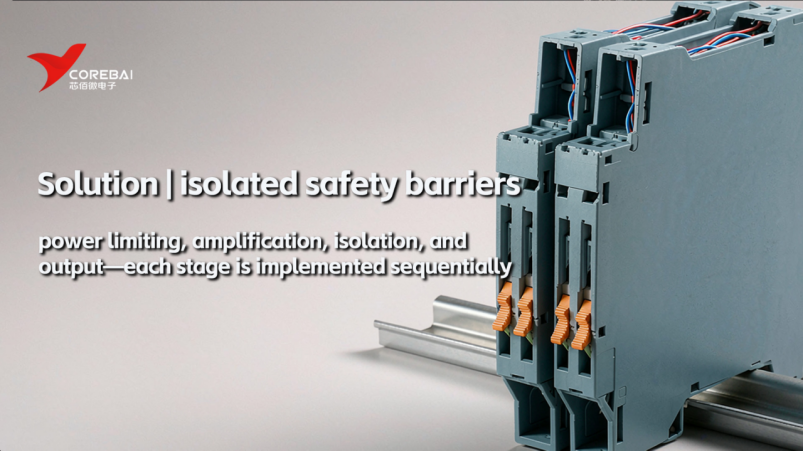
Corebai (COREBAI) has developed a set of domestically produced signal-chain solutions tailored for this device: from signal amplification and buffering on the hazardous side, analog-to-digital conversion, and set-point output, to isolated transmission, 4–20 mA reconstructed output, isolated power supply, and system reset monitoring—each stage offers corresponding domestically produced components as options. The power-limiting unit belongs to the intrinsically safe circuitry of the complete device and is implemented by the system manufacturer during system design. The chips in this solution support the amplification, conversion, isolation, and output stages following power limiting, serving as a reference for complete-device engineers. At the certification level, the subject of assessment remains the complete device; whether it passes the assessment depends on the system design verification conducted by the device manufacturer.
Overall System Architecture
First, determine the location of the safety barrier within the overall machine circuit:
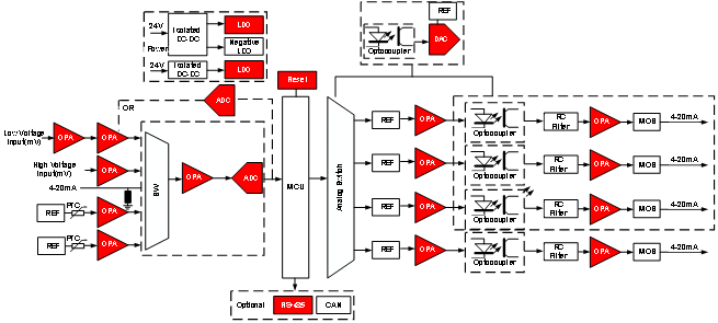
Figure 1: System-level view of the safety barrier transmitter circuit system; image source: Corebai safety barrier isolation technology documentation.
The mV signal and the 4–20 mA loop signal from the field side are multiplexed (via a MUX) and conditioned using operational amplifiers before entering the ADC. The MCU processes the data and, via analog switches, configures the output reference voltage through the DAC. The four 4–20 mA outputs are ultimately reconstructed through operational amplifiers, optocouplers, RC filtering, and MOSFETs. The power supply is derived from a 24 V input and distributed via an isolated DC-DC converter and an LDO; RS-485/CAN communication is optional. The CBM809 is responsible for power-on reset monitoring.
Focusing on the device itself, the structure of an isolated safety barrier can be divided into four sections: the hazardous-side interface, the signal processing unit, the isolation unit, and the safe-side output and power supply.
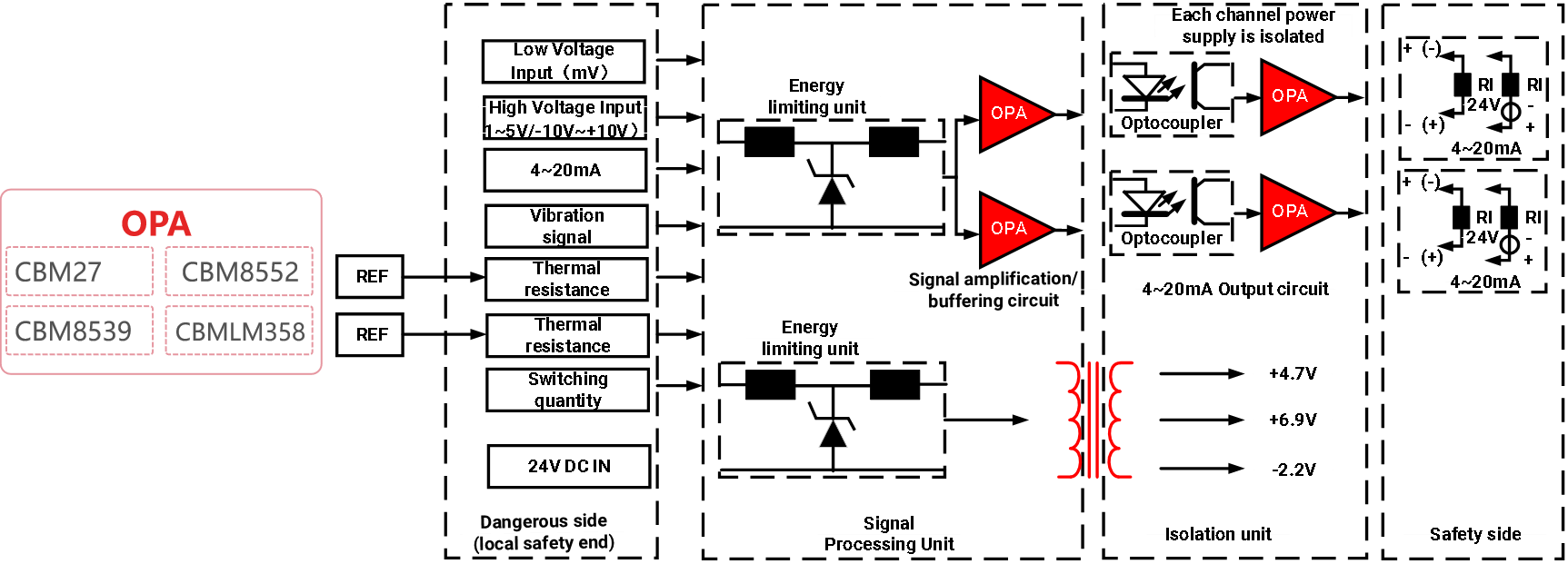
Figure 2: Isolation structure of the safety barrier body; image source: Corebai safety barrier isolation barrier technical documentation.
The signals entering the hazardous side are diverse in type and vary widely in amplitude—ranging from weak millivolt-level signals to high-voltage signals of ±10 V, as well as the 24 V DC power supply provided for two-wire transmitters. All inputs first pass through energy-limiting units, which restrict the energy entering the hazardous side to a safe range. After amplification, buffering, and isolation via optocouplers, the 4–20 mA output is reconstructed on the safe side. The transformer-isolated power supply provides isolated power rails such as +4.7 V, +6.9 V, and-2.2 V. The energy-limiting units are part of the device's intrinsically safe circuitry and are designed and implemented by the device manufacturer; the chip-level solution described below begins with the signal-processing stage following energy limitation.
Module 1: Signal Amplification and Buffering — The Foundation of Accuracy in Analog Front Ends
The signal amplitude downstream of the power-limiting unit is low, and the source impedances vary. The operational amplifier in the first stage determines the fundamental accuracy of the entire system. In the safety-gate channel, this stage typically performs voltage amplification, buffering, and level adaptation. Five domestically produced operational amplifiers are available for selection at this stage—these five are not simply alternative options; instead, they are assigned specific roles based on signal type and accuracy level.
l CBM27A-a precision metering stage, suitable as the first amplification stage for weak mV-level signals
The typical offset voltage is 10 μV, with a maximum of 26 μV; the typical temperature drift is 0.2 μV/°C. After amplification of low-level signals by this device, the error introduced by the offset can be considered essentially negligible at the output. The CBM27G model in the same family offers a lower-performance option with an offset voltage of 100 μV (max) and a temperature drift of 0.4 μV/°C; channels where budget sensitivity is a concern may choose this lower-performance option.
Input noise: 0.09 μVp-p (0.1–10 Hz), 3.0nV/√Hz@1kHz. When amplifying millivolt-level signals such as those from thermocouples and resistance temperature detectors, the noise floor does not obscure genuine variations.
Typical gain-bandwidth product of 8 MHz and a slew rate of 2.8 V/μs, combined with a CMRR of 115–130 dB and an open-loop gain of 950–1800 V/mV.
Supply voltage range: ±4 V to ±18 V (8 V to 36 V); under a 600 Ω load, a ±10 V swing is guaranteed.
Long-term drift: 0.2 μV/month; the calibrated accuracy can be maintained without frequent calibration during the major overhaul cycle of the device.
l CBM8552-zero-drift mode, suitable for wide-temperature-range, single-power-supply measurement channels that require bandwidth.
The chopping stabilization structure features a typical offset voltage of 1 μV and a maximum offset voltage of 5 μV; the typical temperature drift is 0.005 μV/°C, and the cumulative drift error over the wide temperature range is very small.
The typical input bias current is 50 pA; when connected to a voltage-dividing network with high source impedance or to a thermoresistor, the bias error introduced is small.
The typical gain-bandwidth product is 5 MHz, with a slew rate of 1.9 V/μs and a quiescent current of 640 μA per amplifier. Power consumption is higher than that of the CBM8539 and CBMLM358; in exchange, this device offers these bandwidth and drift performance characteristics—making it suitable for the primary measurement channel where drift sensitivity is critical and power consumption is less of a concern.
Both CMRR and PSRR are in the range of 105–132 dB; common-mode interference and power-supply fluctuations on-site are suppressed within the amplification stage.
2.7–5.5 V single-supply, rail-to-rail input/output, MSOP-8/SOP-8 package
l CBM8539-Dual-channel, low-voltage, single-power-supply mode, suitable for intermediate-stage buffering and pre-conditioning in densely populated board cards.
The offset voltage is typically 5 μV and up to a maximum of 15 μV; the typical drift is 0.03 μV/°C; the voltage noise is 1.2 μVp-p (0.1–10 Hz). The accuracy remains essentially unchanged when connected to an ADC driver or when used for pre-amplification and conditioning by an MCU.
The CMRR ranges from 115 to 135 dB, and the open-loop gain ranges from 110 to 130 dB; both the common-mode rejection ratio and the gain margin meet the precision-grade level. The maximum offset of 15 μV is not a limiting factor.
The gain-bandwidth product is 430 kHz, and the slew rate is 0.4 V/μs; the system is capable of adequately processing slowly varying process variables within the safety barrier.
Dual-channel integration: the typical quiescent current per amplifier is 170 μA (maximum 210 μA). It is compatible with a single-supply voltage range of +2.7 V to +5.5 V (±1.35 V to ±2.5 V also supported) and integrates seamlessly with 3.3 V/5 V digital power domains. The device is packaged in SOP-8/MSOP-8 packages and operates within an industrial temperature range of –40 °C to +125 °C. One channel functions as an amplifier and the other as a buffer; a single device covers two stages.
l CBMLM358-a general-purpose, low-cost model suitable for non-precision applications such as digital signal shaping and auxiliary comparison functions.
The typical out-of-spec voltage is 0.4 mV, with a maximum of 5 mV; it is suitable for applications with moderate accuracy requirements, such as threshold detection and digital signal shaping.
Gain-bandwidth product of 1 MHz, slew rate of 0.4 V/μs, quiescent current of 250 μA per amplifier, and low power consumption.
A wide-range, single-supply voltage range of 3–24 V, with a low-output level close to ground (VOL = 5–20 mV); in a single-supply system, the output can directly provide a level close to 0 V.
Dual-channel SOP-8/MSOP-8, with a low-cost tier. Application limitations to note: the operating temperature range is-25 to +80 °C; these devices should not be used in the main measurement channels where wide-temperature requirements apply.
l CBM2904-wide-voltage single-power-supply configuration, suitable for 24 V-class auxiliary circuits and interface adaptation
Power supply: 3–32 V (or ±1.5 V–±16 V); the common-mode input range includes ground potential, allowing single-supply signals referenced to 0 V to be processed directly.
The maximum offset voltage is 9 mV (5 mV at 25 °C), the drift is 7 μV/°C, and the open-loop gain ranges from 15 to 25 V/mV. It is suitable for auxiliary functions such as signal comparison, level shifting, and feed-forward circuit monitoring.
The output swing ranges from 0 V to VCC–1.5 V; with a 30 V supply and a 2 kΩ load, the output can reach 26 V, making it suitable for high-level interface adaptation.
Dual-channel integration; operating temperature range: –40 to +105 °C. The bandwidth parameters for this device are not explicitly specified; its use is not recommended in high-speed applications.
The selection criteria for these five components can be summarized as follows: For the main channel, assess accuracy; for mV-level signals, choose either the CBM27A or the CBM8552 (the former offers greater accuracy margin, while the latter has a temperature drift approximately 40 times lower, features a single-supply rail-to-rail operation, and provides a 5 MHz bandwidth suitable for conventional process signal conditioning). For the intermediate-stage buffering and pre-amplification on densely packed board cards, select the CBM8539; for digital signal shaping and auxiliary circuits, choose the CBMLM358 or the CBM2904. The choice among these options should be determined based on the accuracy requirements of each channel and the cost budget; there is no "all-in-one" combination approach.
Module 2: Analog-Digital Conversion — The Backbone of Multi-Channel Centralized Acquisition
When the safety barrier is designed with a digital architecture, the signals from each channel are aggregated and amplified via a MUX; thereafter, an ADC is required to convert the analog signals into data that the MCU can process. The challenge in this stage lies not in speed, but in the input range and the number of channels.
l CBM76AD06-an 8-channel synchronous sampling data acquisition system designed specifically for industrial voltage ranges.
16-bit, 8-channel synchronous sampling, with a throughput rate of 200 kSPS per channel: multiple field signals can be acquired on a single chip, eliminating the need for a separate ADC for each channel.
The true bipolar input range is ±10 V and ±5 V. When used with an input buffer having an input impedance of 1 MΩ, industrial-standard voltage signals can be connected directly without the need for an additional attenuation network.
The analog input clamp-protection feature can withstand ±16.5 V; in the event of incorrect field wiring or surge intrusion, there is a buffer margin at the front end—this point is particularly relevant to the input terminals of the safety barrier.
The chip integrates a second-order anti-aliasing filter, a 2.5 V precision reference voltage, and reference buffering (reference temperature drift: ±10 ppm/°C); it features an SNR of 95.5 dB, a THD of-107 dB, and INL/DNL of ±0.5 LSB. It offers interfaces compatible with SPI/QSPI/MICROWIRE/DSP and supports flexible parallel/serial configuration.
5 V single-power-supply, power consumption of 100 mW (standby: 25 mW), analog input with a rated 7 kV ESD protection level, LQFP-64 package
The rationale for selecting this solution can be summarized in one sentence: protection, filtering, reference voltage generation, and signal acquisition are integrated into a single chip; consequently, the analog section of the safety barrier channel board consists only of the amplification stage and the power-limiting unit.
Module 3: Benchmark Setting and Adjustment — The DAC delivers the "set value" to the digital side.
In a digital safety barrier, the MCU needs to provide programmable analog setpoints for the output circuit, alarm thresholds, or transmitter excitation; this function is performed by the DAC. The two options should be selected based on the required number of channels and precision specifications.
l CBM53D24-4-channel, 12-bit, single-reference voltage, synchronous update
It features four-channel buffered voltage outputs, with rail-to-rail output amplifiers integrated within the design. The output range is from 0 V to VREF, and it directly drives the output-stage driver circuit.
With a typical INL of ±2 LSB and a typical DNL of ±0.2 LSB, and monotonicity guaranteed, when used as the reference for setting the output loop, the code value corresponds one-to-one to the output.
Single-power-supply operation from 2.5 to 5.5 V; power consumption of 500 μA at 3 V; four channels support synchronous updating; 3-wire serial interface compatible with SPI/QSPI/MICROWIRE/DSP; maximum clock frequency of 30 MHz.
The reset output returns to zero (0 V) upon power-up; during device reboot, the output circuit is not pulled to the hazardous setpoint—this feature is particularly useful in safety-related circuits.
MSOP-10/QFN-10 small package, -40 to +105°C
l CBM128S085-8-channel, 12-bit, with dual-reference independent configuration
A single-chip, 8-channel voltage-output DAC with output buffering; it features rail-to-rail output and offers twice as many channels as the 53D24, making it suitable for models with numerous output circuits and multiple alarm-setting points.
Two external reference inputs supply channels A–D and E–H, respectively, with independent configuration; different circuits may use different ranges.
INL ±2LSB, DNL ±0.2LSB; monotonicity is guaranteed; typical setup time is 6 μs.
Power supply voltage: 2.7–5.5 V; no-load static current: 540 μA @ 3 V / 600 μA @ 5 V; three-wire serial interface with a maximum frequency of 40 MHz, supporting daisy-chaining; multiple DACs can share a single interface set, and wiring remains uncompromised when expanding the number of channels.
TSSOP-16/QFN-16 package, I/O voltage range of 1.8–5.5 V, directly connected to low-voltage MCUs.
The selection process is also simple: for four-channel output, choose CBM53D24; for eight-channel output, or when dual-range zoning is required, choose CBM128S085.
Module 4: Isolation Unit — The optocoupler handles signal transmission across the barrier.
The isolation unit is the core component of the safety barrier. The signal from the hazardous side is transmitted to the safe side entirely via optocouplers, in the form of optical signals. The power supplies for each channel are independent of one another; therefore, any voltage disturbance on the hazardous side cannot reach the safe side in electrical form. When selecting components, attention should be paid to the number of channels, transmission rate, common-mode transient immunity, and isolation voltage rating. The type and number of optocouplers must be determined in accordance with the overall isolation strategy of the system: whether digital signal isolation is used, whether analog signals are digitized via an ADC before isolation, or whether analog signals are transmitted directly via optocouplers. The specific model numbers are not indicated in this block diagram; this article does not specify component part numbers.
Synchronous processing on the power-supply side: After the 24 V input undergoes isolated DC-DC conversion, the transformer transfers the energy to the other side of the isolation barrier, generating isolated power rails such as +4.7 V, +6.9 V, and-2.2 V for use by the operational amplifiers and drive circuits in the output stage. The isolated power supply and the signal isolation share the same layout principles: creep distances and electrical clearances are evaluated in accordance with the design specifications for the entire device, and component placement is organized around the isolation barrier zones.
Module 5: Output Stage and Local Power Supply — 4–20 mA Reconstruction and Low-Voltage Distribution
The safety-side output stage consists of an operational amplifier, an RC filter, MOSFETs, and a V/I conversion circuit. It reconstructs the isolated signal into a 4–20 mA current signal and sends it to the control system. The MOSFETs and optocoupler driver perform the switching and transmission functions in this stage; the block diagram does not specify component models or part numbers. The requirements for the operational amplifier at this stage are output swing and driving capability. The ±10 V swing (600 Ω) of the CBM27A and the wide-voltage output of the CBM2904 are both suitable for this application.
The secondary-side power rail after isolation requires further step-down and waveform shaping to provide clean, low-voltage power to the analog and digital circuits:
l CBM1117-0.8 A linear regulator with local shaping of the power rail after isolation
The output current can reach up to 0.8 A, with fixed output voltages of 1.5/1.8/2.5/3.3/5.0 V and an adjustable range (with a 1.25 V reference).
The output voltage accuracy is ±2%, and the typical load regulation is 0.2%, providing a stable DC operating point for the downstream ADC, DAC, and MCU.
Features built-in current limiting and overheating protection; the device self-limits in the event of an output short circuit or abnormal load.
Typical voltage drop: 1.27 V @ 100 mA (maximum 1.35 V); suitable for stepping down from 5 V/6.9 V rails to the 3.3 V level. This voltage drop does not represent a low-dropout mode: stepping down directly from 24 V to 3.3 V is not feasible; a DC-DC pre-step-down conversion is required first.
SOT-223/TO-252 package, operating temperature range of –40 to +125 °C; a minimum of 10 μF of capacitance must be connected at the output terminal to maintain output stability.
Module 6: Reset Monitoring — Enabling the MCU to be reliably restarted in the event of a power supply anomaly
If the power-up sequence of the MCU in the safety barrier is disrupted, the setpoints in the output circuit and the communication status become unreliable. The reset monitoring mechanism uses a small component to manage this situation:
l CBM809-A streamlined configuration with push-pull reset output and power-supply monitoring
Seven reset threshold levels are available as options (typical values: 2.32/2.63/2.93/3.08/4.00/4.38/4.63 V). Select the corresponding level based on the MCU power domain; the threshold tolerance is in the range of ±1% to ±2%.
Push-pull low-level effective RESET output: no external pull-up required; the reset level is clean.
Maintain the reset pulse after power-on: typically 240 ms (minimum specification: 140 ms), and only release the MCU once the power supply has stabilized. The reset output remains active when the power supply drops to 1 V, preventing the MCU from entering an unreliable operating state under low-voltage conditions.
Quiescent current: 17 μA (typical); SOT-23/SC70 small package; it occupies almost no area when placed at the power input.
The Core Value of the Solution
From an engineer's perspective, the value of this solution lies in the fact that, at every stage, the domestically produced components have parameters that can be queried, and the different performance tiers are clearly differentiated: the precision-grade components (CBM27A/CBM8552/CBM8539) and the general-purpose components (CBMLM358/CBM2904) are allocated according to channel positioning; components corresponding to data acquisition, setting, power supply, and timing are provided for each function. At the board level, the components are primarily packaged in SOP/MSOP/QFN/LQFP formats, and the power supply is compatible with 3.3 V and 5 V power domains.
From the perspective of decision-makers, safety barriers are multi-channel, project-based batch-delivered isolation devices. Operational amplifiers, ADCs, DACs, and power components account for a relatively high proportion of the BOM and represent the primary focus of domestic substitution efforts. Corebai's product portfolio covers five categories: operational amplifiers, ADCs, DACs, LDOs, and monitoring circuits. Within the same supplier framework, the main components of the signal chain can be consolidated—for instance, through centralized quotation requests, certification tracking, and inventory management—thereby reducing supply chain management costs. Delivery lead-time fluctuations for analog devices are common in the industry; however, the domestic supply system can offer more predictable outcomes in terms of localized support and batch continuity. The design, which incorporates multiple grades of operational amplifiers, also allows system manufacturers to allocate costs according to product model tier: high-end models can use precision-grade components, while cost-effective models can use general-purpose grades, eliminating the need for the entire product line to rely on the same expensive imported component.
Another prerequisite that runs throughout the entire system deserves clarification: the overall accuracy of the safety barrier is determined collectively by multiple factors, including energy-limiting voltage drop, amplification, conversion, and V/I conversion matching. The parameters of individual devices are merely necessary conditions; channel-level calibration remains the conventional method for system-wide calibration.
Typical scenarios
Connection of two-wire transmitters in chemical plant equipment: The 24 V power supply on the hazardous side is delivered to the field transmitter via an energy-limiting unit. The returned 4–20 mA loop signal is sampled and amplified (using CBM27A/CBM8552), then acquired by the ADC (CBM76AD06) and isolated via an optocoupler before the output is regenerated on the safe side. The CBM53D24 provides alarm threshold setting.
Thermistor temperature measurement circuit: The thermistor and PTC open-circuit detection signals are amplified by two stages of operational amplifiers before entering the acquisition channel. The low noise and low offset of the CBM27A directly determine the temperature measurement resolution in this channel.
Vibration and multi-channel auxiliary-parameter monitoring: After energy limiting, the multi-channel vibration and auxiliary signals are buffered by the CBM8539 dual-channel buffer; a single chip covers both channels, allowing the channel board area and overall power consumption to remain at relatively low levels. After digitization, the signals are isolated and transmitted to the safety side, where they are processed by the monitoring system for vibration analysis.
Digital signal isolation and multi-channel 4–20 mA output cabinet: The digital signals are shaped by the CBMLM358 and isolated via optical coupling; the multi-channel output reconstruction is handled by the CBM128S085, which provides eight-channel configuration and transmits the data via RS-485/CAN to the control system.
Quick Selection Reference
|
Signal chain location |
Recommended Models |
key parameter |
remarks |
|
Measurement of the main-channel amplification (mV level) |
CBM27A |
Offset: 26 μV (max); noise: 0.09 μVp-p; GBW: 8 MHz (typ); supply voltage: ±4–±18 V |
The greatest accuracy margin is available; the TRIM can be adjusted to zero. |
|
Measurement of main-channel amplification (sensitive to wide-temperature drift) |
CBM8552 |
Offset: 5 μV (max); temperature drift: 0.005 μV/°C (typ); operating voltage: 2.7–5.5 V |
Zero drift, 5 MHz, dual-channel |
|
Intermediate-level buffering/pre-amplification for dense-channel board cards |
CBM8539 |
Offset: 5 μV (typ)/15 μV (max), GBW: 430 kHz, 170 μA/amplifier |
3–5 V power-domain integration with dual-channel integration |
|
Digital signal shaping/auxiliary comparison |
CBMLM358 |
Offset: 5 mV (max), GBW: 1 MHz, single-supply voltage: 3–24 V |
-25 to +80°C; avoid the wide-temperature main channel. |
|
Wide-voltage auxiliary circuit/interface adaptation |
CBM2904 |
Power supply voltage: 3–32 V; common-mode output includes ground; output swing: 0 V to VCC–1.5 V |
Dual-channel; bandwidth not specified; not suitable for high-speed operation. |
|
Multi-channel ADC acquisition |
CBM76AD06 |
16-bit, 8-channel synchronous operation; ±10 V/±5 V input; 200 kSPS; built-in 2.5 V reference voltage |
Clamping-protection voltage: ±16.5 V; operating temperature range: -40 to +85 °C |
|
Output/Threshold Setting DAC (4 channels) |
CBM53D24 |
12-bit, INL of ±2 LSB (typical), resets to zero upon power-on reset, 30 MHz serial interface |
Simultaneous updates across four channels |
|
Output/Threshold Setting DAC (8 channels) |
CBM128S085 |
12-bit, 8-channel, independently configurable with dual reference voltages, 40 MHz daisy-chain interface |
-40~+125℃ |
|
Local LDO after isolation |
CBM1117 |
0.8 A, ±2% accuracy, differential pressure: 1.27 V @ 100 mA (typ.) |
Current-limiting overheating protection requires coordination with DC-DC pre-reduction. |
|
MCU reset monitoring |
CBM809 |
Seven threshold levels: 2.32–4.63 V; typical reset pulse width: 240 ms (lower limit: 140 ms); static current: 17 μA |
Push-pull low-effective-output configuration |
The circuitry of an isolated safety barrier is not particularly complex; the real challenge lies in simultaneously managing energy limitation on the hazardous side, signal accuracy, electrical isolation, and power-supply timing. The competitiveness of this type of equipment is determined by two factors: the system design capabilities for isolation and energy limitation, combined with a stable, controllable material supply chain with appropriately configured stages. This solution organizes the safety-barrier signal chain into six stages: energy limitation, amplification, conversion, isolation, output, and monitoring. Energy limitation is handled by the integrated energy-limiting unit; each of the remaining five stages incorporates domestically produced components with verifiable parameters and defined operating boundaries. The operational amplifiers are divided into five stages according to channel accuracy; the CBM76AD06 integrates the acquisition link into a single chip; the DACs are selected in two stages based on the number of output channels; and the CBM1117 and CBM809 address power supply and timing requirements, respectively.。The suite provided by Corebai is intended for complete equipment manufacturers to use progressively, based on the specific model and its positioning, in the product design of isolated safety barriers; system-level verification in the intrinsically safe design of the complete equipment should still be assessed in accordance with the requirements for complete equipment specified in the relevant certification system.
010-62106066
( Monday to Friday 9:00 - 18:00 )
 704-705, Block D, Building 2, No. 9 Fenghao East Road, Haidian District, Beijing

Wechat Public Account


This app respects and protects the privacy of all users who use the service. In order to provide you with more accurate and personalized services, this app will use and disclose your personal information in accordance with this Privacy Policy. However, this application will treat this information with a high degree of diligence and prudence. Except as otherwise provided in this Privacy Policy, this application will not disclose or provide this information to third parties without your prior permission. This app will update this privacy policy from time to time. By agreeing to this Application Services Use Agreement, you are deemed to have agreed to the entire content of this Privacy Policy. This Privacy Policy is an integral part of this Application Service Agreement.


 Online Store
 A/D Converters (ADC)
 RF Transceiver
 Controller
 Power Management
 Logic gates
 Real-time clocks
 Digital Isolator
 Darlington Transistor
 D/A Converters (DAC)
 Sensors
 Analog Switches Multiplexers
 Interface
 Monitoring Circuit
 Amplifier


 在线商城
