

 Released:2026-11-12 14:04:38
 Views 38 次
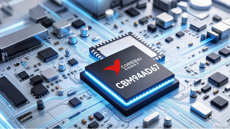
 CBM94AD67是芯佰微的一款16位单片中频采样ADC,最高采样率250MSPS,面向无线接收器、仪器及测试设备等对高速采样和动态性能有较高要求的应用。产品提供CBM94AD67-200与CBM94AD67-250两个速度等级,采用DDR LVDS数字输出并支持SPI配置,可应用于通信、接收器、基站、宽带无线、雷达、光谱分析等场景。 【核心亮点抢先看】 ▶ 16 位| 最高 250MSPS -200最高200MSPS,-250最高250MSPS;在170MHz输入、250MSPS条件下

The CBM94AD67 is a 16-bit single-chip intermediate-frequency sampling ADC from Corebai Micro, featuring a maximum sampling rate of 250 MSPS. It is designed for applications—such as wireless receivers, instruments, and test equipment—that demand high-speed sampling and excellent dynamic performance. The product is available in two speed grades, CBM94AD67-200 and CBM94AD67-250; it utilizes DDR LVDS digital outputs and supports SPI configuration, making it suitable for applications in communications, receivers, base stations, broadband wireless systems, radar, spectral analysis, and other scenarios.
[Key Highlights at a Glance]
▶ 16-bit | Up to 250 MSPS
-200: up to 200 MSPS; -250: up to 250 MSPS. Under an input of 170 MHz and at 250 MSPS, the typical SNR for-250 is 72.03 dBFS, and the SFDR is 89.05 dBc.
▶ 60 fs RMS jitter | 900 MHz full-power bandwidth
Typical aperture jitter is 60 fs rms, with a full-power bandwidth of 900 MHz, providing the necessary bandwidth foundation for the acquisition of broadband intermediate-frequency signals.
▶ DDR LVDS | Flexible SPI Configuration
It features an ANSI-644-compliant DDR LVDS output and provides a DCO data clock, an OR over-range indicator, and multiple SPI configuration functions; it also supports parameter adjustments for output format, test mode, drive current, and other settings.
Product Positioning and Speed Class
Q1: What type of ADC is the CBM94AD67, and what are its core specifications?
A: The CBM94AD67 is a 16-bit single-chip mid-band sampling ADC with a maximum sampling rate of 250 MSPS. The product features differential analog inputs with a maximum analog input range of 2.5 Vpp; during operation, it requires 1.8 V and 3.3 V power supplies as well as a differential input clock. The digital side provides DDR LVDS outputs and a DCO data clock. The product is housed in a QFN-72 package and operates within a temperature range of −40 °C to +85 °C.
Selection guidance: Its primary application is high-speed intermediate-frequency signal acquisition. If the system places greater emphasis on low-speed acquisition or DC accuracy, product selection should be based on the specific sampling rate, bandwidth, and accuracy requirements.
Q2: How should you choose between the CBM94AD67-200 and the CBM94AD67-250?
A: The difference between the two ranges lies in the sampling rate and the typical dynamic range: the sampling rates are 50–200 MSPS and 50–250 MSPS, respectively;
The two variants have identical static electrical specifications, including INL, DNL, offset error, and gain error; their guaranteed lower limits for SNR, SFDR, and ENOB are also consistent. At the same input frequency, typical dynamic specifications exhibit only minor differences. Taking an input frequency of 170 MHz as an example, the typical SNR values are 71.82 dBFS and 72.03 dBFS, while the typical SFDR values are 89 dBc and 89.05 dBc, respectively.
Selection guidance: Prioritize selecting the speed class based on the system's required maximum sampling rate, rather than simply pursuing an even higher sampling rate.
Q3: Which applications does it target? Is it suitable for my use case?
A: The application scope spans nine categories: communications, receivers, base stations, spectral analysis, broadband wireless communications, radar, infrared imaging, power-amplifier linearization, and image processing. These scenarios share the common feature of feeding high-and mid-frequency signals directly into an ADC, thereby eliminating one stage of mixing.
Implementation note: High-frequency broadband acquisition (broadband reception, radar, and spectral analysis) best leverages its bandwidth and dynamic range; low-speed acquisition, which primarily relies on DC accuracy, is not its primary application area.
Dynamic Performance and Static Accuracy
Q4: How do SNR and ENOB perform at different input frequencies?
A: Under 250 MSPS sampling conditions, as the input frequency increases, both SNR and ENOB decrease slightly. Taking the-250 version as an example:
|
incoming frequency |
SNRrepresentative value |
ENOBrepresentative value |
|
70MHz |
74.42dBFS |
12.04bit |
|
140MHz |
72.75dBFS |
11.76bit |
|
170MHz |
72.03dBFS |
11.65bit |
The corresponding guaranteed lower limits are 70 dBFS, 69 dBFS, and 69 dBFS, respectively; the guaranteed ENOB lower limits are 11.2 bits, 11 bits, and 11 bits, respectively.
Q5: How does SFDR perform, and what does strong adjacent-band interference imply?
A: Under 250 MSPS conditions, the typical SFDR values for the-250 version at 70 MHz, 140 MHz, and 170 MHz inputs are 91.31 dBc, 89.04 dBc, and 89.05 dBc, respectively; the corresponding guaranteed lower limits are 77 dBc, 75 dBc, and 75 dBc, respectively.
SFDR is used to describe the difference between the fundamental component and the largest spurious component. For receiving systems containing strong interfering signals, SFDR is one of the key metrics that should be emphasized when evaluating ADC spectral performance.
Q6: How should the DNL and INL indicators be interpreted?
A: For the CBM94AD67, the typical DNL is ±0.5LSB and the typical INL is ±3.5LSB, with the test condition set at a 10 MHz input. The guaranteed ranges are DNL −1 to 1.5LSB and INL −16 to 16LSB, respectively.
Design note: Typical values and guaranteed ranges should be distinguished from one another. In systems with stringent requirements for absolute conversion accuracy, an assessment should be conducted in light of the specific application conditions.
Q7: To what extent can the imbalance and gain error be corrected?
A: The typical offset error for the CBM94AD67 is −5 LSB, and the typical gain error is −1.8% FSR. The SPI provides an Offset adjustment function; additionally, the input full-scale range can be configured via the Vref register, supporting 2.0 Vpp–2.5 Vpp, with a default value of 2.5 Vpp.
Engineering note: If the system has higher requirements for overall conversion accuracy, the device adjustment functionality can be integrated with a system-level calibration scheme in the design.
Digital Interface and SPI Configuration
Q8: What digital output interface does the CBM94AD67 use?
A: The CBM94AD67 features a DDR LVDS digital output and is compatible with ANSI-644; it also provides a DCO data clock output and an OR over-range indication. The data output consists of multiple sets of differential data pairs, and the DCO can be used in conjunction with the receiving end for data acquisition timing design.
Design tip: When designing a high-speed digital interface, the overall design should integrate the DCO timing, PCB routing, and the receiving-end capture window.
Q9: What functions can be configured on the SPI?
A: SPI allows configuration of multiple operating parameters, including:
l Internal shutdown mode
l Clock Duty Cycle Stabilizer
l stochastic pattern
l Output test mode
l BIST
l Enter full-scale range
l Enter AC/DC coupling mode
l Offsetadjust
l Output data format
l Output drive current
l DCO phase, output delay, etc.
In addition, the output test mode provides test data including the median value, positive/negative full-scale values, checkerboard patterns, PN23, PN9, and 1/0 alternation, which can be used for high-speed digital link debugging.
Q10: Can the output drive current be adjusted? What are the benefits of lowering it?
A: Yes. The output drive current supports multi-level adjustment, with a range of 1.71 mA to 3.0 mA; the default value is 3.0 mA.
Design note: Gear selection should be based on an analysis of trace length and receiver sensitivity; for long traces or high loads, the lowest gear should not be selected.
Clock and Front-End Design
Q11: What are the requirements for the clock input?
A: The ADC uses differential clock inputs and provides an internal 0.8 V common-mode voltage; the external clock should be AC-coupled. The minimum differential input clock amplitude is 250 mVpp, compatible with LVDS/LVPECL levels; the maximum allowable single-ended amplitude is VCM ± 0.9 V. The input clock duty cycle should be maintained at 50 ± 5%; three drive schemes—balun, LVPECL, or LVDS—may be used.
Q12: Why do high-speed ADCs place particular emphasis on clock jitter?
A: High-speed ADCs are relatively sensitive to clock jitter, particularly when the input signal frequency is high. The aperture jitter of the CBM94AD67 is 60 fs rms (typical); the relationship between SNR and jitter is given by SNR = 20×lg(1/(2π×fIN×tjitter)). The higher the input frequency, the greater the amount of SNR consumed by a given amount of jitter. To maintain optimal SNR under high-frequency analog input conditions, the system clock jitter should be less than 100 fs.
Design note: In actual system design, the clock source, clock distribution, and jitter introduced by the PCB should be incorporated into the overall clock budget, and the design should be evaluated in conjunction with the target input frequency.
Q13: How should the analog input front end be designed?
A: The CBM94AD67 employs a differential analog input. To achieve good dynamic performance, the manual recommends matching the source impedance at the differential analog terminals and connecting a small resistor in series at the input; additionally, a low-Q inductor or ferrite bead and a matching capacitor network should be configured according to the input frequency to reduce noise and parasitic effects. For inputs below approximately 150 MHz and for inputs ranging from 150 MHz to 300 MHz, the manual provides recommended input networks for each case, respectively.
Engineering note: For high-speed intermediate-frequency sampling systems, the performance of the ADC itself constitutes only one part of the signal chain; the front-end drive, matching, and filtering networks must likewise be designed in conjunction with the target frequency.
On-site Troubleshooting for the Data Collection Chain
Q14: After powering on, no data can be acquired; where should I look for the issue?
A: You can perform the inspection in the following sequence: "power supply → clock → SPI configuration → digital output."
First, verify whether the 1.8 V and 3.3 V power supplies are functioning properly, as well as whether the CLK± differential clock is operating correctly; next, check the SPI configuration to ensure that the system has not entered a full-chip power-off or output power-off state. The CBM94AD67 supports multiple output test modes; you can first use the test data to verify the digital output link, and then proceed to inspect the analog inputs and peripheral circuits.
Q15: The output data occasionally exhibits jumps or bit errors; how can the issue be localized?
A: Priority should be given to checking the digital interface timing, DCO phase and delay, output drive current, and PCB trace conditions. The CBM94AD67 supports DCO phase and output delay adjustment, as well as multiple output drive current configurations, enabling fine-tuning in accordance with different digital interface conditions.
[Selection Summary]
The core advantage of the CBM94AD67 lies not merely in its "16-bit, 250 MSPS" capabilities, but in the integration of high-speed sampling, wideband input, dynamic performance, and a high-speed digital interface. The two speed grades, -200 and-250, cover sampling requirements up to 200 MSPS and 250 MSPS, respectively; under 170 MHz input and 250 MSPS conditions, the-250 version achieves a typical SNR of 72.03 dBFS and an SFDR of 89.05 dBc, along with a typical rms aperture jitter of 60 fs and a full-power bandwidth of 900 MHz.
010-62106066
( Monday to Friday 9:00 - 18:00 )
 704-705, Block D, Building 2, No. 9 Fenghao East Road, Haidian District, Beijing

Wechat Public Account


This app respects and protects the privacy of all users who use the service. In order to provide you with more accurate and personalized services, this app will use and disclose your personal information in accordance with this Privacy Policy. However, this application will treat this information with a high degree of diligence and prudence. Except as otherwise provided in this Privacy Policy, this application will not disclose or provide this information to third parties without your prior permission. This app will update this privacy policy from time to time. By agreeing to this Application Services Use Agreement, you are deemed to have agreed to the entire content of this Privacy Policy. This Privacy Policy is an integral part of this Application Service Agreement.


 Online Store
 A/D Converters (ADC)
 RF Transceiver
 Controller
 Power Management
 Logic gates
 Real-time clocks
 Digital Isolator
 Darlington Transistor
 D/A Converters (DAC)
 Sensors
 Analog Switches Multiplexers
 Interface
 Monitoring Circuit
 Amplifier


 在线商城
