

 Released:2026-11-11 13:15:22
 Views 110 次
 CBM14AD125Q 是芯佰微的 4 通道 14 位 125MSPS 流水线模数转换器:1.8V 单电源供电,串行 LVDS 输出,48 引脚 QFN-48 封装,工作温度 −40℃~+85℃,面向医疗成像、高速成像、无线电接收机与便携式测量设备这类多通道采集系统。

The CBM14AD125Q is a 4-channel, 14-bit, 125 MSPS pipelined analog-to-digital converter from Corebai Micro: it operates on a single 1.8 V power supply, provides serial LVDS output, features a 48-pin QFN-48 package, and operates in a temperature range of −40 °C to +85 °C; it is intended for multi-channel acquisition systems used in medical imaging, high-speed imaging, radio receivers, and portable measurement devices.
[Key Highlights at a Glance]
▶ 4-channel synchronous acquisition; 14-bit, up to 125 MSPS; SNR 77 dBFS (9.7 MHz, VREF = 1.3 V)
▶ SFDR: 86 dBc (VREF = 1.3 V) / 91 dBc (VREF = 1.0 V); both values are specified up to the Nyquist frequency
▶ 1.8 V single power supply, 125 MHz mode: ≤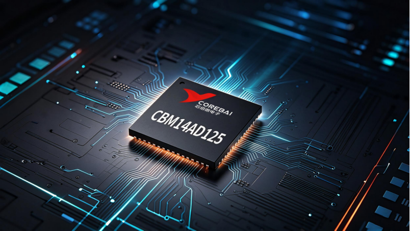
195 mW per channel; typical <14 mW after disabling all channels
▶ 650 MHz full-power analog input bandwidth; sampling clock compatible with LVPECL/CMOS/LVDS
Sampling Architecture and Dynamic Performance
Q1: What order of magnitude does 4-channel, 14-bit, 125 MSPS, SNR 77 dBFS represent?
A: This is a multi-channel pipelined ADC with four independently sampled channels; the conversion rate can be configured from 20 to 125 MSPS. Dynamic performance is listed in two tiers based on reference conditions: with VREF = 1.3 V, the SNR is 77 dBFS (for a 9.7 MHz input); with VREF = 1.0 V, it is 75 dBFS. When comparing dynamic performance with similar devices, it is essential to align the reference conditions with the input frequency—digital values under the two different references correspond to their respective test conditions; comparing them under mismatched reference conditions is meaningless.
Q2: SFDR provides two values, 86 dBc and 91 dBc; which one should be used for the assessment?
A: The two values correspond to two reference configurations: at VREF = 1.3 V, the value is 86 dBc; at VREF = 1.0 V, it is 91 dBc; both are specified at the Nyquist frequency. In these two sets of results, the SNR at the level one above the SFDR is 75 dBFS; whether this relationship holds under other conditions and frequency bands should be determined by actual measurements in the target frequency band. The reference level should follow the system's primary requirements: for a multi-channel receiving front-end sensitive to spurious signals, the 1.0 V level may be used instead of 91 dBc; for a system prioritizing noise floor, the 1.3 V level should provide 77 dBFS.
Q3: DNL ±0.6LSB and INL ±5.0LSB—what does this imply for the accuracy budget?
A: Differential nonlinearity of ±0.6 LSB results in control within ±1 LSB, with uniform inter-symbol transitions; integral nonlinearity of ±5.0 LSB corresponds to approximately 0.03% of full scale and is the dominant factor affecting static accuracy. In AC-coupled dynamic acquisition, the influence of INL is primarily manifested in harmonic components; when performing DC or low-frequency precision measurements, the ±5 LSB should be incorporated into the error budget together with offset and gain errors before determining whether the budget is adequate. The actual lower limit of accuracy for a 14-bit system is typically determined jointly by INL and reference drift; relying solely on the number of resolution bits will overestimate the accuracy.
Clock Input and Multi-Chip Synchronization
Q4: Which signal types does the sampling clock support? Does it require an external bias?
A: LVPECL, CMOS, and LVDS-compatible signals are all acceptable; a sinusoidal clock can also be used. The clock input pin is internally biased, so an external biasing circuit is unnecessary; the signal is typically AC-coupled to CLK+/CLK− via a transformer or capacitor. For optimal performance, a differential clock is recommended; a single-ended signal can be converted to differential using an RF balun or a transformer. Specifically, for clock frequencies ranging from 125 MHz to 1 GHz, a balun solution is recommended; for 40–200 MHz, a transformer solution is recommended. The secondary side can be connected across a Schottky diode to limit the clock to approximately 0.8 V peak-to-peak differential, which both blocks high-amplitude feedthrough and preserves fast edges.
Q5: If the input clock duty cycle is not the standard 50%, will performance be affected?
A: In typical high-speed ADCs, two clock edges generate an internal timing signal, making the design sensitive to the duty cycle; generally, a ±5% tolerance is required. This part incorporates a built-in duty-cycle stabilizer (DCS) that re-timed the non-sampling edges to generate an internal clock with a nominal duty cycle of 50%; once enabled, it significantly improves the noise and distortion performance for duty-cycle inputs ranging from 30% to 45% and from 55% to 70%. Additionally, note that when the clock rate changes dynamically, the DCS loop requires 1.5–5 µs to reacquire lock; therefore, variable-speed systems should include this interval in their switching wait time. The jitter of the rising edge itself is not managed by the DCS; consequently, the quality of the clock source must still be controlled independently.
Q6: How can multiple ADCs achieve synchronous sampling?
A: Built-in input clock divider supporting integer multiple division from 1 to 8; an external SYNC input is provided to reset and align the clock dividers of each chip, helping multiple chips align their sampling instants. The final alignment depends on the clock distribution and SYNC timing; therefore, multi-chip systems should be designed and verified in accordance with the required timing specifications. The register also allows the user to configure whether the system should be resynchronized each time a SYNC is received, or only upon the first synchronization.
Analog Input and Reference Configuration
Q7: How should a 650 MHz input bandwidth be used in conjunction with an input range of 2.0 Vp-p to 2.6 Vp-p?
A: First, let's clarify a common misconception: 650 MHz is the full-power bandwidth specification for the analog input path; it is not equivalent to the sampling rate—the upper sampling rate limit is 125 MSPS. These are parameters from two different dimensions. The engineering significance of a 650 MHz bandwidth lies in the fact that this component can directly sample high-and medium-frequency signals (via undersampling); the input range is determined by the reference voltage configuration: VREF = 1.0 V corresponds to a full-scale input of 2.0 Vp-p, while VREF = 1.3 V corresponds to 2.6 Vp-p; the register also provides five additional subdivision levels (1.0/1.14/1.33/1.6/2.0 Vp-p), with the 1.3 V reference configured at 1.3× the corresponding level. When configuring the system, the reference mode and register level should be confirmed together. Once the input range is exceeded, performance deteriorates sharply; therefore, a margin should be reserved in the front-end amplitude based on the selected level. In undersampling applications, wide bandwidth is a double-edged sword: the front-end RC network and the filter must suppress broadband noise outside the target bandwidth; otherwise, the noise floor will be sampled along with the desired signal.
Q8: What are the different configuration options for the reference voltage?
A: The SENSE pin supports three operating modes via its voltage divider configuration: when grounded, it uses the internal 1.0 V reference; when connected to an external resistor divider, VREF = 0.5 × (1 + R2/R1), with the requirement that 7 kΩ ≤ R1 + R2 ≤ 10 kΩ; when connected to AVDD, the internal reference is disabled and an external reference voltage (1.0–1.3 V) is used, in which case the internal reference buffer acts as a 7.5 kΩ load. It is not recommended to leave the SENSE pin unconnected. The VREF pin should be bypassed to ground in parallel with low-ESR 1.0 µF and 0.1 µF capacitors. Sharing a common reference across multiple channels can improve gain matching between channels; in this case, the internal reference's load capability must be taken into account.
Q9: What is the best method for driving the analog front end?
A: Differential drive. For baseband applications, a differential balun can be used to provide flexible interface options; for applications where SNR is a critical parameter, differential transformer coupling is recommended, since the noise performance of most amplifiers is insufficient to match the true dynamic performance of this component. Single-ended input driving is not recommended. When using AC coupling, the input terminal has no internal DC bias; it must therefore be externally biased to VCM = AVDD/2, with the VCM pin bypassed to ground via a 0.1 µF capacitor. The front-end RC network can be configured according to the frequency band: for 0–100 MHz, use R1 = 10–33 Ω, C1 = 5 pF, R2 = 1 5 Ω, and C2 = 1 5 pF; for 100–300 MHz, use 10 Ω, 5 pF, 10 Ω, and 10 pF. When driving high-frequency signals, it is recommended to reduce or remove the series differential capacitor C1.
Power Consumption Management and Serial Output
Q10: How is power consumption calculated when all four channels are fully enabled?
A: In 125 MHz mode, power consumption per channel does not exceed 195 mW; when all four channels are fully enabled, the total power consumption can be calculated by summing the consumption of each channel. Power consumption is also proportional to the sampling rate, so downsampling can further reduce power consumption. Channels that are not currently in use can be independently powered off via SPI; after all channels are disabled, typical power consumption is less than 14 mW. When budgeting power consumption for a portable device, use the number of enabled channels multiplied by 195 mW as the upper limit, then account for the impact of the sampling rate setting; only then can the margin be accurately determined.
Q11: What is the difference between power-saving mode and standby mode?
A: Power-saving mode can be entered by using SPI or by setting the PDWN pin high; the typical power consumption is 2 mW, the output driver enters a high-impedance state, and the internal reference voltage source, reference buffer, bias network, and clock are all turned off. The wake-up time depends on the duration of the power-saving mode: the shorter the sleep time, the faster the wake-up. In standby mode, the internal reference voltage circuit remains powered, which is useful in scenarios requiring rapid recovery. Systems that use time-shared sampling and require rapid recovery should select standby mode; systems that require long periods of sleep and prioritize power savings should select full power-off mode. Additionally, PDWN uses the digital output driver power supply (DRVDD) as its reference; its level must not exceed that of this power supply.
Q12: What configuration options are available for the LVDS output?
A: The output complies with the ANSI-644 LVDS standard, with an output current of 3.5 mA and a swing of 350 mV under a 100 Ω terminated load. The serial output supports various combinations of SDR/DDR, single-channel/dual-channel, and bit-by-bit/byte-by-byte modes; the output format can be selected as offset binary or binary two's complement, with MSB-first as the default; additionally, a data clock output (DCO) and a frame clock output (FCO) are provided for downstream acquisition. In terms of timing: transmission delay is 2.3 ns, output rise/fall times are 300 ps, and the data output duty cycle is 50%.
Q13: What functions can be configured on the SPI?
A: The three-SPI interfaces (SCLK/SDIO/CSB) cover the primary operating states: power modes (normal operation / complete power-off / standby), clock division ratio, duty-cycle stabilizer switching, output format and termination, and so on; they also include built-in digital test codes—fixed test codes (positive/negative full-scale, alternating checkerboard, etc.), PN23/PN9 pseudo-random sequences, and custom user test codes configured via SPI. When debugging the acquisition link, first apply a fixed code or a PN sequence to verify the LVDS channel and downstream decoding; then switch back to the actual signal, which will greatly accelerate problem localization.
On-site investigation of sampling anomalies
Q14: The noise floor is too high, and the SNR is clearly below the nominal level; where should I start investigating?
A: The root cause should first be attributed to clock quality. The typical aperture jitter for this component is 135 fs rms; mid-band undersampling applications are particularly sensitive to clock jitter, and excessive jitter directly raises the noise floor and compresses the dynamic range. Troubleshooting sequence: confirm that the clock source is a low-jitter crystal oscillator or a low-jitter clock driver; separate the clock driver's power supply from the ADC output driver's power supply to prevent digital noise from being mixed into the clock; for clocks obtained through gating or frequency division, use the original clock for final retiming. Treating the clock input as an analog signal during routing and processing is often the first corrective step for this type of issue.
Q15: If no data is received from the LVDS output, or if the data bits are misaligned, how can the issue be localized?
A: Attribute the issue to three possible causes. First, the correspondence between the sample and the output has not been accounted for in the pipeline delay: the data lags the simulated input by approximately 16 clock cycles; misalignment of the capture window manifests as a mismatch between the data content and the input sample—this is a bit-level issue, not a link fault. Second, synchronization and alignment issues: when the SYNC timing in a multi-chip system is not met, the frequency divider is not properly aligned; after a speed change, the DCS loop requires 1.5–5 µs to reacquire lock, during which the output should not be trusted. Third, termination and format configuration: when there is absolutely no data on the LVDS line, this layer should be checked first—verify that the 100 Ω differential termination, output format, and bit-order settings are consistent with those used for decoding at the receiving end. A common practice is to first switch the output to a built-in fixed test pattern to verify the link; once the fixed pattern passes, check the synchronization and timing of the actual signal.
Q16: The input signal amplitude is not large, yet the code values frequently approach full-scale; what could be the cause?
A: There are two common causes. First, the input range setting does not match the reference configuration: the input range depends on the reference voltage setting; when the input range is set to a narrow range while the front-end signal is designed for a wide range, the peak will be clipped, and performance will deteriorate sharply once the range is exceeded—transient out-of-range conditions can be recovered after just one clock cycle, whereas sustained out-of-range conditions require adjustment of the front-end amplitude. Second, the common-mode bias is incorrect: in AC-coupled applications, if the input is not biased to VCM = AVDD/2, common-mode out-of-range conditions likewise manifest as abnormal code values. It is recommended to first use a meter to verify whether the voltages at the VCM and VREF pins match the expected values, and then verify the upper input amplitude limit corresponding to that range setting.
[Selection Summary]
The CBM14AD125Q uses a single 1.8 V power supply to acquire 4-channel, 14-bit, 125 MSPS data with an SNR of 77 dBFS and a power consumption of ≤195 mW per channel, packaged in a QFN-48 package. Multi-chip synchronization, independent channel shutdown, and a built-in test code provide a ready-made pathway for the setup and debugging of multi-channel systems. When selecting a part, determine the reference level based on the system's primary requirements (prioritize the 1.3 V level if noise floor is the primary concern, or the 1.0 V level if spurious noise suppression is the priority); verify the undersampling strategy against the clock jitter budget; and then perform a power consumption budget based on the number of channels to be enabled. Completing these three steps allows you to determine whether the part qualifies for BOM consideration.
[Quick Specification Reference]
|
project |
specifications |
|
Channel / Resolution |
4 channels / 14 bits |
|
transformation rate |
20~125MSPS |
|
supply electricity |
1.8V single power supply |
|
presentation of information |
Serial LVDS (ANSI-644) |
|
Full-power analog input bandwidth |
650MHz |
|
Packaging / Operating Temperature |
QFN-48 / −40℃~+85℃ |
010-62106066
( Monday to Friday 9:00 - 18:00 )
 704-705, Block D, Building 2, No. 9 Fenghao East Road, Haidian District, Beijing

Wechat Public Account


This app respects and protects the privacy of all users who use the service. In order to provide you with more accurate and personalized services, this app will use and disclose your personal information in accordance with this Privacy Policy. However, this application will treat this information with a high degree of diligence and prudence. Except as otherwise provided in this Privacy Policy, this application will not disclose or provide this information to third parties without your prior permission. This app will update this privacy policy from time to time. By agreeing to this Application Services Use Agreement, you are deemed to have agreed to the entire content of this Privacy Policy. This Privacy Policy is an integral part of this Application Service Agreement.


 Online Store
 A/D Converters (ADC)
 RF Transceiver
 Controller
 Power Management
 Logic gates
 Real-time clocks
 Digital Isolator
 Darlington Transistor
 D/A Converters (DAC)
 Sensors
 Analog Switches Multiplexers
 Interface
 Monitoring Circuit
 Amplifier


 在线商城
