
 Released:2025-08-06 09:41:02
 Views 1743 次
 本文聚焦CBM3232低功耗RS-232收发器,从技术背景出发,阐述其应对RS-232通信挑战的核心定位,进而深入解析其产品架构、功能模块、关键参数,探讨典型电路设计、封装布局细节,并强化可靠性防护措施,同时展现多领域应用场景的适用性,并补充测试验证与问题解决方案。全文基于实测数据,为工程设计提供从芯片特性到实际部署的精简技术参考。

This paper focuses on the CBM3232 low-power RS-232 transceiver. Starting with technical background, it elaborates on its core positioning in addressing RS-232 communication challenges. The analysis delves into product architecture, functional modules, and key parameters, while exploring typical circuit designs and packaging layout details. Enhanced reliability protection measures are introduced to demonstrate applicability across multiple fields, complemented by test verification and troubleshooting solutions. Based on practical measurement data, this comprehensive study provides concise technical references for engineering design, covering chip characteristics through real-world deployment.
As a serial communication standard established by EIA/TIA, RS-232 is widely used for short-distance data transmission between devices. Its core requirement is to enable bidirectional conversion between TTL/CMOS voltage levels (0~3.3V) and RS-232 standard levels (±3V~±15V). With the development of industrial automation, portable devices, and IoT technologies, traditional RS-232 transceivers are increasingly facing three major technical challenges:
l Low power demand: battery-powered handheld terminals, medical hand-held devices and other scenarios require the static current of the chip to be controlled in mA level to extend the battery life;
l Anti-interference capability: In industrial workshops and consumer electronics plug-in scenarios, electrostatic discharge (ESD) and electromagnetic interference (EMI) are easy to cause communication interruption, so the protection design needs to be strengthened;
l Environmental adaptability: A wide temperature range of-40℃~85℃ and small size packaging (to accommodate high density PCB) are the basic requirements for industrial equipment.
In this context, with the rapid development of industrial automation, medical equipment, and power systems, there has been a significant increase in demand for stable and reliable communication interfaces. RS-232 transceivers featuring low power consumption, high ESD protection, wide temperature adaptability, and flexible packaging have become essential market requirements. CBM3232, designed by Corebai Micro as a high-performance solution, meets these urgent demands for premium RS-232 transceivers.
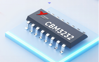
The Corebai CBM3232 is a dual-channel RS-232 level conversion chip compliant with EIA/TIA-232 and V.28/V.24 standards. Featuring an integrated charge pump voltage converter, driver/receiver module, and enhanced ESD protection network, it is optimized for low-power, high-reliability applications. Key advantages include: 1) Typical current of just 2.5mA at 3.3V supply; 2) Supports 120Kbps high-speed transmission; 3) Withstanding ±15kV air discharge and ±8kV contact discharge; 4) Operating across-40℃ to 85℃ temperature range; 5) Available in SOP-16 and TSSOP-16 packaging options. This versatile solution perfectly meets level conversion requirements in industrial control, portable devices, medical electronics, and consumer electronics.
l Key parameters and performance characteristics

The core architecture consists of the following modules:
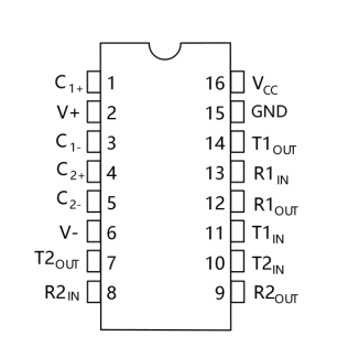
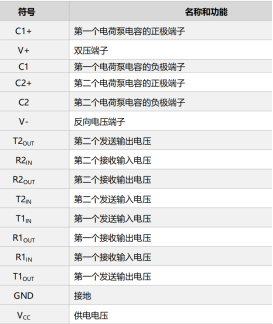
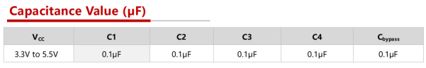
The voltage conversion from ±5V to ±10V is achieved through four 0.1μF external capacitors (C1-C4), supporting dual power inputs of 3.3V/5V. The charge pump circuit adopts a symmetrical design to ensure stable output voltage, providing the required positive and negative voltages for RS-232 standard levels.

(2) Driver and receiver module
l Two receivers (R1IN/R2IN): support a wide input range of ±25V, low threshold value (VRIL) is 0.6V and high threshold value (VRIH) is 1.5V when powered by 3.3V, and built-in 0.3V hysteresis voltage to suppress noise interference.
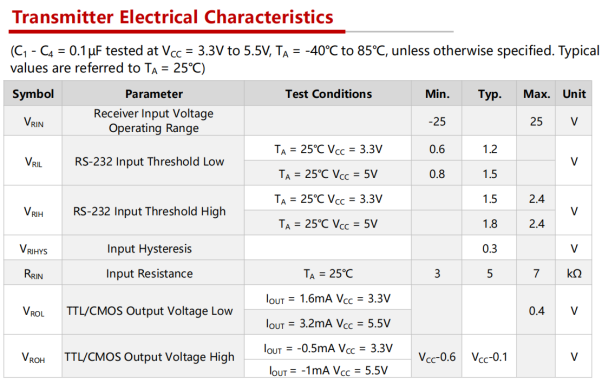
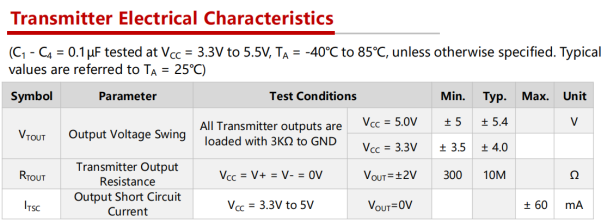
l Two drivers (the output swing reaches ±3.5V~±4.0V (3kΩ load when powered by T1OUT/T2OUT):3.3V), supporting 120Kbps high-speed data transmission, and the compression rate is ≥3V/μs to ensure that the signal edge is steep without trailing.
(3) ESD protection network
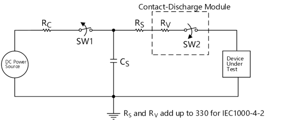
All I/O pins are integrated with multi-stage diode clamping structure, which complies with IEC61000-4-2 standard, and can withstand ±15kV air discharge and ±8kV contact discharge, effectively resisting the damage of human static electricity or environmental transient discharge to the chip.
3、Circuit design specifications: from basic links to anti-interference optimization practices
3.1 Basic communication circuit
Four 0.1μF ceramic capacitors (C1-C4) and one 0.1μF bypass capacitor are required. T1IN/T2IN connects to the TTL level output of the MCU, while R1OUT/R2OUT connects to the RS-232 interface, forming a complete level conversion chain.
When cascading multiple chips, it is recommended to use chrysanthemum chain topology. SYNC pins of each chip should be shared with ground to ensure phase consistency. The test shows that the phase deviation can be controlled within 5ns when cascading four chips.
l The power supply pin (VCC) is connected in parallel with 10μF tantalum capacitor +0.1μF ceramic capacitor to form a π type filter network, which can effectively suppress the generation of power supply ripple.
l The ground plane is designed to be segmented, and the analog ground and digital ground are connected at a single point to reduce the possibility of noise coupling.
4、Packaging and PCB layout: physical implementation strategy adapted to the scenario
The chip offers two packaging options:
SOP-16: Pin spacing 1.27mm, overall size 9.80~9.98mm (length) × 5.80~6.20mm (width), suitable for manual welding and prototype development stage, especially suitable for industrial control cabinets and other equipment with less strict volume requirements.

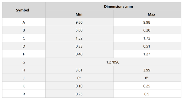
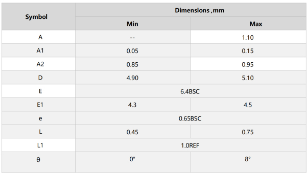
TSSOP-16: Pin spacing 0.65mm, size 4.90~5.10mm (length) × 6.40mm (width), volume is about 40% smaller than SOP-16, suitable for high-density PCB layout of portable devices (such as handheld data acquisition terminal).

Signal partition: The charge pump circuit (C1+/C1-, C2+/C2-) and transmitter output (T1OUT/T2OUT) are divided into separate regions to avoid digital signal interference with analog voltage conversion.
Grounding design: GND pin should be connected to the PCB ground plane through more than 4 vias. The ground plane is copper plated, and the analog ground and digital ground are connected at a single point (it is recommended to use 0Ω resistance) to prevent noise caused by ground potential difference.
Walking line rules: Send/receive signal line width ≥0.2mm, length ≤10cm, differential pair spacing ≥3 times the line width to reduce crosstalk.
All I/O pins of the chip are integrated with multi-stage diode clamping circuit, and ESD protection class complies with IEC61000-4-2 standard:
Air discharge: ±15kV (driver output, receiver input pin);
Contact discharge: ±8kV.
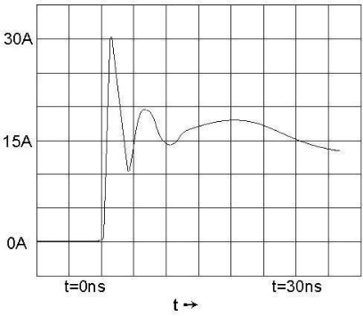
ESD test waveform
Interface protection: In the T1OUT/R1IN signal lines of RS-232 interface, SMBJ33ATVS diodes are connected in parallel. The clamping voltage is less than or equal to 33V, the response time is less than 1ns, and transient overvoltage is absorbed.
Isolation design: In the environment with strong interference such as motor and frequency converter, RS-232 isolation module (such as ADuM3160 with 2.5kV isolation) should be used to avoid ground loop interference.
In industrial automation systems, the CBM3232 serves as a communication bridge between PLCs and sensors/actuators. For instance, in smart production line material sorting systems, it converts TTL signals from PLC outputs to RS-232 standard levels to drive data transmission for conveyor belt encoders. The device operates reliably across-40℃ to 85℃ temperature ranges, adapting to both high-temperature and low-temperature workshop environments. Its enhanced electrostatic protection resists static interference from frequent equipment insertion and removal, with air discharge tolerance reaching ±15kV and contact discharge tolerance up to ±8kV. The maximum transmission rate of 120Kbps meets real-time control command requirements, while its compact design with SOP-16 packaging enables high-density layout on industrial control boards.
In battery-powered portable devices such as handheld data acquisition terminals, the typical operating current during communication with barcode scanning modules under 3.3V power supply is only 2.5mA, significantly extending the operational duration of the 1000mAh lithium battery. The compact TSSOP-16 package (length 4.90~5.10mm) occupies merely 2% of the terminal PCB space, fully meeting modern equipment's urgent demand for miniaturization. Additionally, its receiver supports a wide input range of ±25V, compatible with output levels of various scanning modules, thereby reducing the design complexity of peripheral adaptation circuits.
Medical handheld devices require stringent reliability and anti-interference performance. The portable ECG monitor features ±8kV contact discharge protection during heart rate data transmission to the host unit, effectively preventing electrostatic damage during medical procedures. Its 3V/μs voltage swing rate ensures sharp signal edges and reduces waveform distortion from electromagnetic interference. With a wide temperature range of-40°℃ to 85°℃, it adapts to extreme conditions in ambulances, operating rooms, and other environments. Additionally, its simplified peripheral circuit design using only four 0.1μF capacitors significantly streamlines sterile packaging processes.
In consumer electronics such as printers and smart home controllers, the CBM3232 addresses interface level adaptation challenges. For example, in household printers, it enables RS-232 communication between the main control chip and PC, delivering 120Kbps transmission rates that meet document printing command requirements. Operating at 3.3V with a ±3.5V~±4.0V output swing, it seamlessly integrates with PC RS-232 interface standards. Its enhanced electrostatic discharge protection (with ±15kV air discharge capability) accommodates frequent USB-to-RS-232 cable reconnections, while the SOP-16 package featuring 1.27mm wide pin spacing significantly simplifies soldering operations during mass production.
Use a digital multimeter to measure:
Driver output voltage: ±3.5V±0.2V when powered by 3.3V.
Receiver input impedance: 3kΩ~7kΩ.
Observe through the oscilloscope:
Eye test: at 120Kbps rate, eye height is ≥2.5V and eye width is ≥4μs.
Overcharge/bell: the output signal overshoot is ≤10%, and the bell amplitude is ≤5%.
Check whether the power supply voltage is stable at 3.3V±5%.
Measure whether the voltage across C1-C4 capacitor reaches ±5V, which is an important sign of normal operation of charge pump.
The oscilloscope captures the output waveform of the driver to confirm whether there is signal distortion.
If ESD damage occurs, the following steps can be used to locate it:
Use a multimeter to detect I/O pin short circuit to ground.
When replacing the damaged chip, replace the ESD protection capacitor (0.1μF) at the same time.
The following accelerated aging tests are recommended:
High temperature storage: 1000 hours at 85℃.
Temperature cycle: -40℃~85℃,1000 cycles.
Humidity test: 85%RH, 85℃ environment storage for 500 hours.
The internal structure of the chip is examined by X-ray fluoroscopy, and the fault point is located by flying needle test.
010-62106066
( Monday to Friday 9:00 - 18:00 )
 704-705, Block D, Building 2, No. 9 Fenghao East Road, Haidian District, Beijing

Wechat Public Account

This app respects and protects the privacy of all users who use the service. In order to provide you with more accurate and personalized services, this app will use and disclose your personal information in accordance with this Privacy Policy. However, this application will treat this information with a high degree of diligence and prudence. Except as otherwise provided in this Privacy Policy, this application will not disclose or provide this information to third parties without your prior permission. This app will update this privacy policy from time to time. By agreeing to this Application Services Use Agreement, you are deemed to have agreed to the entire content of this Privacy Policy. This Privacy Policy is an integral part of this Application Service Agreement.
 A/D Converters (ADC)
 RF Transceiver
 Controller
 Power Management
 Logic gates
 Real-time clocks
 Digital Isolator
 Darlington Transistor
 D/A Converters (DAC)
 Sensors
 Analog Switches Multiplexers
 Interface
 Monitoring Circuit
 Amplifier
 在线商城
在线商城