
 Released:2025-07-30 10:44:15
 Views 2030 次
 在5G基站、宽带传输等场景中,如何用单芯片实现多载波信号的高保真转换?芯佰微CBM97D79TQ作为一款双通道16位高动态范围数模转换器(DAC),凭借1GSPS采样速率、80dBc邻道泄漏比(ACLR)及低功耗特性,成为宽带通信发射链路的核心解决方案。本文从核心性能、设计要点到工程落地,详解其技术优势与实践指南。 一、应用技术背景介绍 在无线通信与宽带传输随着5GNR、WiMax等技术的广泛普及,系统对高带宽、低失真以及多载波并发能力的需求愈发迫切: 带宽需求:5G基站需支持S

In 5G base stations and broadband transmission scenarios, how can a single chip achieve high-fidelity conversion of multi-carrier signals? The CBM97D79TQ dual-channel 16-bit high dynamic range digital-to-analog converter (DAC) from Corebai Micro stands out as a core solution for broadband communication transmission links, featuring 1GSPS sampling rate, 80dBc adjacent channel leakage ratio (ACLR), and low power consumption. This article delves into its technical advantages and practical implementation guidelines, covering key performance aspects, design considerations, and engineering deployment.
With the widespread adoption of 5GNR, WiMax and other technologies in wireless communication and broadband transmission, the system's demand for high bandwidth, low distortion and multi-carrier concurrency capability is becoming more and more urgent:
Bandwidth requirements: 5G base stations need to support the parallel transmission of multi-carrier signals in Sub-6GHz band, and the single carrier bandwidth can reach 100MHz. It is required that the DAC sampling rate exceeds 1GSPS to cover the ultra-wide spectrum;
Signal fidelity: In order to ensure the quality of 5G broadband communication signal, adjacent channel leakage ratio (ACLR) must reach or exceed 80dBc to avoid interference between multiple carriers, which puts forward high requirements for the dynamic performance of digital-to-analog converter (DAC);
Integration and power consumption: Base station AAU (active antenna unit) and other equipment are limited by volume and heat dissipation, which requires DAC not only to have high integration, such as built-in calibration and synchronization functions, but also to have low power consumption characteristics, that is, the power consumption should be controlled below 1.0W@1GSPS.
In addition, in point-to-point broadband transmission scenarios such as LMDS and MMDS, the equipment needs to cover the frequency band of 1GHz and above, while the traditional multi-chip splicing scheme is faced with the problems of large synchronization error and high power consumption, so it is urgent to realize the direct generation of wideband signals by single-chip solution.
CBM97D79TQ is a dual-channel 16-bit high dynamic range digital-to-analog converter (DAC) launched by Corebai Microelectronics. It is designed for broadband communications and wireless infrastructure. Its core advantages are high sampling rate, low power consumption and highly integrated functions. The core features are as follows:
l Sampling rate: Supports the highest sampling rate of 1GSPS, and can generate multi-carrier signals up to the Nyquist frequency, which meets the requirements of "single chip coverage of multiple bands" in broadband communication.
l Spectrum tuning capability: The built-in 2x/4x/8x interpolator and complex modulator can flexibly place the carrier in any position within the bandwidth of the DAC, and can adapt to different frequency band requirements without additional mixer.
l Digital modulation technology: supports real/reverse modulation functions, can directly generate orthogonal modulation signals, simplify the design of base station transmission link.
l Power optimization: The power consumption is only 1.0W@1GSPS and 600mW@500MSPS under full working conditions, which is suitable for heat sensitive base stations and broadband equipment scenarios.
l Signal fidelity:
The adjacent channel leakage ratio (ACLR) of single carrier WCDMA reaches 80dBc@80MHz intermediate frequency, effectively reducing the interference to adjacent channels;
The simulated output current is adjustable (8.7mA~31.7mA), suitable for 25Ω~50Ω loads, and can be directly connected to the ADIADL537XFMOD series modulator.
l The importance of adjustable analog output:
l The output current is programmable and adjustable (10mA to 30mA), enabling the system to dynamically optimize signal amplitude based on load characteristics (e.g., 25Ω/50Ω impedance). This prevents signal-to-noise ratio loss or insufficient drive capability caused by fixed output settings. For example, in 5G base stations, adjusting the output current precisely matches the input requirements of LDMOS power amplifiers, ensuring a balance between linearity and efficiency.
l Auxiliary calibration: 4 auxiliary DAC can directly control the gain and loss of the external VGA, simplifying the front-end circuit calibration process.
l Multi-chip synchronization: The differential synchronization interface (SYNC_I±/SYNC_O±) supports multi-device cascading to meet the requirements of multi-channel expansion such as MIMO transmission diversity.
l Clock management: Built-in high-performance phase-locked loop (PLL) clock multiplier, which can generate low jitter sampling clock and reduce the complexity of external clock source design.
Dynamic performance directly determines the purity of the signal in transmission. The measured data is as follows:
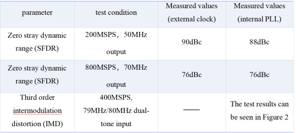
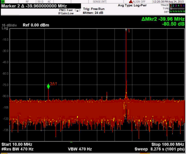
Figure 1: Test results of no stray dynamic range (mid frequency output 70MHz, conversion rate 800MSPS)
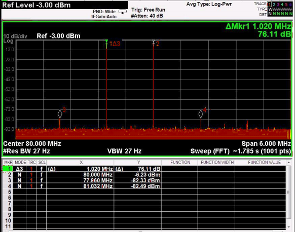
Figure 2: Test results of third-order double tone intermodulation (mid frequency output 79MHz/80MHz, conversion rate 400MSPS)
Static parameters reflect the linear conversion capability of digital signal to analog signal. The typical values of the five chips measured are as follows:
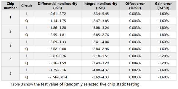
l Microscopic nonlinearities (DNL):-0.61~+2.72LSB (I channel), -1.14~+1.75LSB (Q channel);
l Integral nonlinearity (INL):-2.34~+5.45LSB (I channel), -2.47~+3.85LSB (Q channel);
l Dissimilarity error: 0.003%FSR (typical value), gain error-1.6%FSR (typical value).
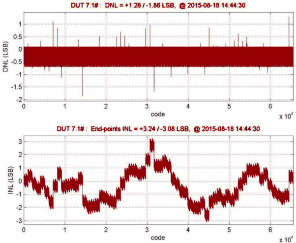
Typical differential nonlinear/integral nonlinear diagram
l Working voltage: 3.3V for analog power supply and 1.8V for digital/clock power supply, compatible with industrial power supply scenarios;
l Working temperature: -40℃~ +85℃, to meet the needs of vehicle and industrial extreme environment;
l Packaging: 100 pin TQFP package (16mm × 16mm), tray packaging (90 pieces per tray).
CBM97D79TQ is functionally divided into five modules:

CBM97D79TQ functional architecture block diagram
l Digital filter unit: responsible for 2x/4x/8x interpolation and digital modulation, supporting complex modulator to flexibly place the carrier within the bandwidth of DAC;
l DAC core unit: 16-bit design, output current can be adjusted (10mA~30mA), using 0.18μmCMOS process to ensure high-speed conversion stability;
l Clock unit: contains PLL multiplier, supports external clock input and internal clock generation, and can suppress the impact of clock jitter on dynamic performance;
l Auxiliary DAC: 2 independent channels are used for external VGA gain and offset correction to simplify the calibration process of analog front end;
l Synchronization unit: The multi-chip synchronization unit is responsible for the synchronization function between multiple chips.
l Output matching: DAC differential outputs (OUT1_P/N, OUT2_P/N) need to match 25Ω~50Ω loads. It is recommended to convert them into single-ended signals through baron conversion before connecting to the RF link. For example, in point-to-point broadband transmission, 50Ω matching can reduce reflection loss and improve signal integrity.
l Interpolation configuration: Select the interpolation multiplier according to the output frequency. For example, 4 times interpolation (800MSPS sampling) is recommended for 70MHz output, and digital anti-sinc filter is used to suppress image interference. The selection of interpolation multiplier should balance the bandwidth requirements and the complexity of digital filter.
l Clock selection: The internal PLL can be enabled when sampling at 200MSPS or above (the PLL_LOCK pin indicates the lock in high level). When sampling at 100MSPS, the external clock is required (the PLL does not support this frequency). The internal PLL can reduce the design cost of the external clock source at high frequency.
"The application object circuit board should be required to separate the digital ground and analog ground as far as possible, and do not lay the digital line next to the analog line or under the DAC." The analog ground (AGND) and digital ground (DGND) should be connected by a single point of 0Ω resistance to avoid digital noise coupling to the analog link.
"The ground of the chip should be connected to the ground layer of the PCB board through as many channels and enough area as possible." It is necessary to design a large area of copper foil under the chip and connect it to the ground layer through multiple holes to enhance the anti-interference ability and heat dissipation effect.
"Input lines should be as short as possible to minimize parasitic capacitance and noise introduction", especially for high frequency signal lines such as clock (REFCLK±) and synchronization (SYNC_I±), which should be short and straight to reduce the influence of parasitic parameters.
Digital data lines (P1D0~P1D15, P2D0~P2D15) shall not pass through the analog area or under the DAC output path to avoid digital signal interference with the analog link.
Although the chip has built-in electrostatic protection structure, "attention should be paid to electrostatic protection during testing, handling and storage", and measures such as grounding bracelet and anti-static packaging should be taken to avoid damage to the circuit by high-energy electric pulses.
l Wireless infrastructure: Base station transmission links such as W-CDMA, GSM, LTE, and 5GNR support multi-carrier signal generation. For example, in wireless base stations, the CBM97D79TQ can directly generate intermediate frequency signals to drive LDMOS power amplifiers. By optimizing the bias voltage through adjustable output current, it ensures PA linearity.
l Broadband communication: LMDS, MMDS, point-to-point broadband transmission, single chip coverage of ultra-wide band. Its 1GSPS sampling rate can support up to 500MHz signal bandwidth, to meet the needs of high-speed data transmission.
l Digital IF synthesis: Direct generation of 70MHz~200MHz IF signal, eliminating the need for traditional mixer. When used with ADI ADL537XFMOD modulator, it can simplify the RF front-end design.
Attachment: CBM97D79TQ [Chinese typesetting] parameter manual
010-62106066
( Monday to Friday 9:00 - 18:00 )
 704-705, Block D, Building 2, No. 9 Fenghao East Road, Haidian District, Beijing

Wechat Public Account

This app respects and protects the privacy of all users who use the service. In order to provide you with more accurate and personalized services, this app will use and disclose your personal information in accordance with this Privacy Policy. However, this application will treat this information with a high degree of diligence and prudence. Except as otherwise provided in this Privacy Policy, this application will not disclose or provide this information to third parties without your prior permission. This app will update this privacy policy from time to time. By agreeing to this Application Services Use Agreement, you are deemed to have agreed to the entire content of this Privacy Policy. This Privacy Policy is an integral part of this Application Service Agreement.
 A/D Converters (ADC)
 RF Transceiver
 Controller
 Power Management
 Logic gates
 Real-time clocks
 Digital Isolator
 Darlington Transistor
 D/A Converters (DAC)
 Sensors
 Analog Switches Multiplexers
 Interface
 Monitoring Circuit
 Amplifier
 在线商城
在线商城