
 Released:2025-08-13 10:25:32
 Views 1584 次
 在雷达、卫星通信等高频信号处理场景中,工程师常面临一个棘手问题:当输入信号频率攀升至400MHz以上时,传统ADC的无杂散动态范围(SFDR)会迅速退化至60dB以下,致使信号中微弱的目标信息被噪声所掩盖——这在卫星通信接收深空微弱信号时,可能直接造成“漏判”或“误判”。 芯佰微电子推出的CBM94AD34-50012位高速模数转换器(ADC),以“高采样率+高动态性能+进口替代兼容性”三大核心优势,成为破解高频信号采集痛点的关键方案。

In high-frequency signal processing applications such as radar and satellite communications, engineers frequently encounter a critical challenge: when input signal frequencies exceed 400MHz, the spurious-free dynamic range (SFDR) of conventional ADCs rapidly degrades below 60dB, causing weak target signals to be overwhelmed by noise——. This phenomenon may directly lead to missed detection or false detection during satellite communication operations when receiving faint deep-space signals.
The CBM94AD34-50012-bit high-speed analog-to-digital converter (ADC) launched by Corebai Microelectronics has become a key solution to solve the pain points of high-frequency signal acquisition with three core advantages: "high sampling rate + high dynamic performance + import substitution compatibility".
In radar, broadband communication and other high-frequency applications, ADC serves as the "first threshold of analog signal to digital signal", and its performance directly determines the accuracy of back-end signal processing. However, traditional solutions have three bottlenecks:
In high-frequency applications, the dynamic performance of ADCs significantly deteriorates. For instance, when the input signal frequency increases from 30MHz to 450MHz, many 12-bit ADCs experience a 8-10dB reduction in their spurious-free dynamic range (SFDR), typically falling below the 65dB performance threshold. This attenuation means that strong signal sidebands may overwhelm weaker signals, as seen in radar systems where a strong reflection target at close range can mask smaller targets farther away.
Sampling rate and power loss: In order to cover broadband signals, ADC needs to support sampling rates above 500MSPS, but the power consumption of traditional solutions is generally more than 1000mW, which will lead to serious heating and sudden reduction of battery life in scenarios with limited power supply such as satellites and UAVs.
Poor compatibility of imported alternatives: Mainstream imported ADCs (such as ADIAD9434) are faced with problems such as long delivery cycle and unstable supply chain, while domestic alternatives often need to redesign the circuit board due to differences in pin definition and timing logic, increasing research and development costs.
CBM94AD34-500 is a 12-bit single-chip analog-to-digital converter (ADC) developed by Corebai Micro, optimized for high performance, low power consumption, and user-friendliness. Manufactured using the SiGeBiCMOS process, it features a 56-pin plastic package (QFN56) and integrates a Sample-and-Hold Amplifier (SHA) with an on-chip reference voltage source, delivering a complete signal conversion solution. The VREF pin supports both internal reference voltage adjustment and external reference input (external reference mode requires activation via the SPI port), enabling flexible adaptation to diverse signal processing requirements.
The product is mainly used in wireless and broadband communications, receivers, communication test equipment, radar and satellite subsystems, and power amplifier linearization scenarios.
Performance parameters: resolution of 12 bits, sampling rate of 500MSPS, no stray dynamic range (SFDR)>65dB, input range can be adjusted between 1.18Vp-p to 1.6Vp-p, and compatible with AD9434 series pins.
Power supply and interface: 1.8V analog power supply is required, differential clock is adopted to ensure the overall performance; digital output is compatible with LVDS (ANSI-644), data format supports binary complement, Gray code or offset binary, and data output clock is provided to ensure accurate timing.
Replacement advantage: It can directly replace ADI's AD9434BCPZ-500 in the United States, and the pin definition and packaging form are consistent, so it is easy to replace quickly.
|
Working frequency (fCLK): ≤500MHz |
|
Analog and digital power supply voltage: 1.75V~1.9V |
|
Simulated input common mode voltage: 1.6V~1.8V |
|
Working environment temperature: -40℃~85℃ |
|
Input signal amplitude peak to peak (VIN(P-P)):≤1.5V. |
|
Disestability error: -5.0mV~+5.0mV, gain error: -9%FS~ +9%FS |
|
Microlinear error (DNL):-1.5 ~ 1.5LSB and integral linear error (INL) : -4.5 ~ 4.5 LSB |
|
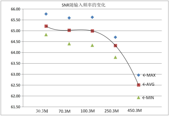
Signal to noise ratio (SNR):30.3MHz input ≥ 63dBFS,450.3MHz input ≥ 61dBFS |
|
Power consumption: typical value ≤900mW, standby power consumption ≤60mW, sleep power consumption ≤12mW |
Figure 1 illustrates the functional block diagram of CBM94AD34, which primarily comprises multiple stages of pipeline architecture (Stages 1-8), buffer and bias circuits, reference buffer circuit, data alignment/control and digital correction circuit, OTP (One-Time Programmable) circuit, clock stabilization and management circuit, control circuit, SPI data format selection and output driver circuit, among other modules. These components work in concert to achieve efficient conversion and processing from analog signals to digital signals. The clock stabilization and management circuit ensures precise sampling clock synchronization, while the SPI interface provides flexible control for data format configuration.
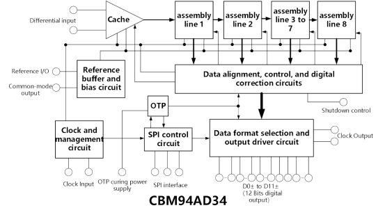
Figure 1 function block diagram
CBM94AD34 is packaged in a 56-pin QFN. Some key pins function as follows:
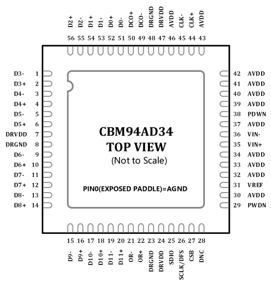
Figure 2 shows the lead arrangement
Differential output pins: include the positive and negative ends of D0-D11 (e.g., D3-at pin 1, D3+ at pin 2, D4-at pin 3, etc.), which are used to output the converted digital signal. The differential form is adopted to improve the anti-interference capability.
Power supply pins: Analog power supply (VCC) is distributed on multiple pins (such as 30,32, etc.), and digital power supply (VDD) includes 7, 24, etc., all of which are powered by 1.8V. Note that the analog power supply and digital power supply should be stabilized.
Control pins: Pin 29 (PWDN) serves as the shutdown mode selection pin, Pin 25 (SDIO) handles SPI data input/output (serial mode), Pin 26 (SCLK/DFS) manages both SPI clock (serial mode) and output format selection (external pin mode), while Pin 27 (CSB) acts as the SPI chip select (low-level active). These pins enable precise control and configuration of the chip's operational modes.
Input pins: VIN+ at pin 35 is the positive end of analog differential input, VIN-at pin 36 is the negative end of analog differential input, CLK+ at pin 44 is the positive end of clock differential input, CLK-at pin 45 is the negative end of clock differential input, and CML at pin 40 is the common mode voltage bias output.
Other pins: 21 OR-and 22 OR+ are the positive and negative ends of overflow judgment bit; 49 DCO-and 50 DCO+ are the positive and negative ends of data clock; 8, 23 and 48 are digital ground (GNDD).
Note: NC terminal (e.g. 28) should be left empty during normal use.
CBM94AD34 achieves optimal performance through differential input configuration, with multiple recommended circuits for different application scenarios:
In baseband applications, the AD8138 differential driver provides excellent performance and flexible interfaces. The AD8138 outputs a common-mode voltage that can be easily set to AVDD/2+0.5V and can be configured as a Sallen-Key filter topology to limit the bandwidth of the input signal. The specific circuit is shown in Figure 3.
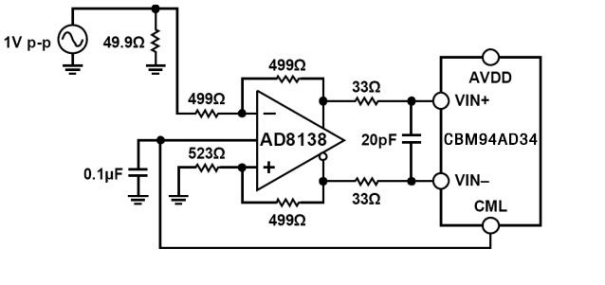
Figure 3 uses the AD8138 for differential input configuration
When the input frequency is in the second or higher Nyquist region, especially for medium frequency under-sampling applications from 70MHz to 100MHz, it is recommended to use a differential dual-barrel coupling input configuration. When selecting the transformer, signal characteristics should be considered to avoid distortion caused by low-frequency saturation and excessive power, as shown in Figure 4.
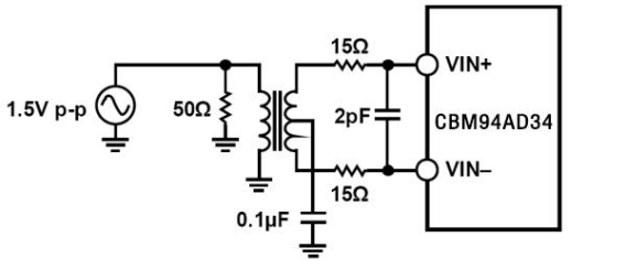
Figure 4 Differential transformer coupling configuration
When the frequency is in the second Nyquist region, the AD8352 differential driver can also be used. The example circuit is shown in Figure 5.
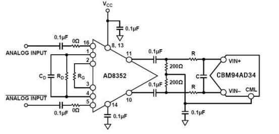
Figure 5 uses AD8352 for differential input configuration
In any configuration, the value of the parallel capacitor C depends on the input frequency and the source impedance, and it may be necessary to reduce the capacitance or remove the parallel capacitor.
In order to make full use of the chip performance, the CBM94AD34 sampling clock input (CLK+) and CLK-) should adopt a differential signal. The following clock input circuit is recommended:
The low-jitter clock source's single-ended signal is converted to a differential signal by using an RF transformer. A back-to-back Schottky diode connected to the transformer's secondary can limit the clock signal to approximately 0.8V peak-to-peak differential, which not only retains the fast rise and fall times, but also prevents the large voltage swing from affecting the low-jitter performance. The circuit is shown in Figure 6.
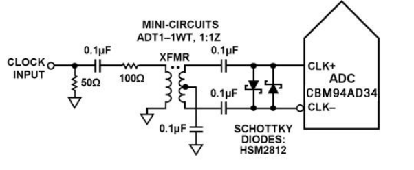
Figure 6 configuration of transformer coupled differential clock
If there is no low jitter clock source, the differential PECL signal can be coupled AC to the sampling clock input pin. The AD9510/AD9511/AD9512/AD9513/AD9514/AD9515 series clock drivers have excellent jitter performance, as shown in Figure 7.
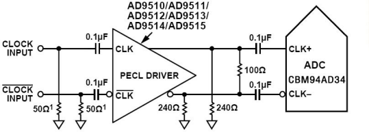
Figure 7 Differential PECL, sampling clock
Alternatively, a differential LVDS sampling clock configuration can be used. The circuit is shown in Figure 8.
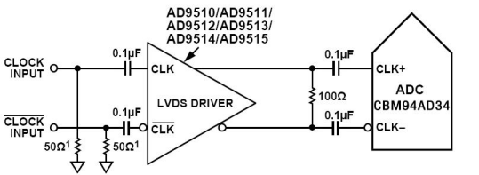
Figure 8 Differential LVDS, sampling clock
In certain applications, a single-ended CMOS signal can drive the sampling clock input. The CLK+ pin is directly driven by the CMOS gate circuit, while the CLK-pin is grounded through a 0.1μF capacitor. When driving CLK+ with a 1.8VCMOS signal, the CLK-pin requires a parallel bias configuration using a 0.1μF capacitor and a 39kΩ resistor. The circuit configuration is illustrated in Figure 9.
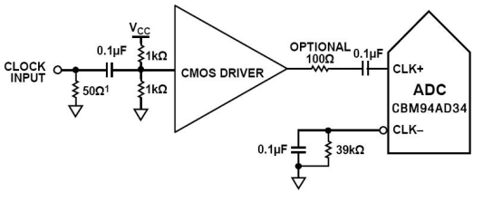
Figure 9 Single-ended 1.8V CMOS, input clock
CLK+ and CLK-pins have an internal bias of approximately 0.9V, without external bias; if the clock signal is coupled DC, the common mode voltage should be kept within the range of 0.9V.
The differential output of CBM94AD34 defaults to the ANSI-644LVDS standard. The data format can be configured via SPI to adopt a low-power, signal-selective format similar to IEEE1596.3 standards, which further reduces power consumption by approximately 39mW. LVDS drivers consist of a current source driving a differential pair, typically operating at 3.5mA. When a 100Ω termination resistor is connected to the LVDS receiver's input, it generates a voltage swing of approximately 350mV.
This LVDS output format is designed for seamless integration with LVDS receivers in custom ASICs and FPGAs, delivering exceptional switching performance in high-noise environments. It is recommended to position the single-point-to-point network topology with a 100Ω termination resistor as close as possible to the receiver. This approach prevents timing errors caused by excessive termination distance or poor differential traces, while ensuring trace lengths do not exceed 24 inches. Differential outputs should be routed in parallel with identical lengths.
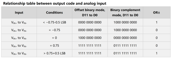
The output data format is offset binary by default, and binary complement, Gray code, etc. are also supported. The relationship between input and output codes and analog input is shown in the table.
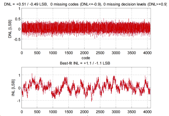
Under the test conditions of sampling rate fCLK=500MHz and input signal frequency fIN=30.3MHz, the differential linear error (DNL) of CBM94AD34 is-0.51/+0.49LSB, with no bit loss (DNL ≤ -0.9) and bit loss decision level (DNL ≥ 0.9); the integral linear error (INL) is-1.1/+1.1LSB.
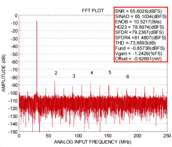
When the sampling rate fCLK=499.99970304MHz and input signal frequency fIN=30.28867830MHz are given, the test results are: SFDR=79.23dBFS, second and third harmonic distortion (HD2,3nd)=78.89dBFS, and fourth harmonic distortion (HD4nd)=81.48dBFS,SNR=65.6dBFS,SINAD=65.1034dBFS,ENOB=10.5217bits.
According to the performance parameters of CBM94AD34 analog-to-digital converter, it has good dynamic performance in broadband applications. The SNR curve with the change of input frequency shows certain changes at 30.3MHz, 70.3MHz, 100.3MHz, 250.3MHz, 450.3MHz and other input frequency points, and the overall level remains high.
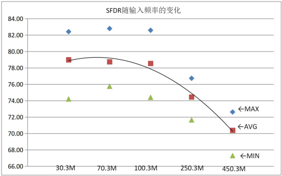
The curve of SFDR with input frequency variation shows that the non-spurious dynamic range has excellent performance under various input frequency conditions, which fully meets the requirements of various broadband applications.
In wireless and broadband communication systems, the CBM94AD34500MSPS sampling rate can meet the real-time digitalization requirements of broadband signals. With 12-bit resolution and SFDR (spurious-free dynamic range) of ≥65dB, it can accurately capture the detailed characteristics of complex modulation signals, which is suitable for the signal acquisition requirements of base station transceiver, satellite communication ground station and other equipment.
As the core component of receivers, the CBM94AD34 features a wide input range (1.18Vp-p to 1.6Vp-p), enabling compatibility with signals of varying intensities. Its differential input architecture and anti-interference design (LVDS output and differential clock) effectively suppress noise, ensuring accurate conversion of weak signals such as long-distance communication signals and radar echoes. This makes it widely applicable in various communication receivers and radar receiver front-ends.
For radar and satellite subsystems, CBM94AD34's high dynamic performance (SFDR≥72dBFS@30.3MHz) can distinguish strong and weak target signals, its wide temperature operating range of-40℃~85℃ can adapt to extreme environments, and its differential clock design ensures the timing stability of high-speed sampling. It plays a key role in weather radar, phased array radar and spaceborne data transmission systems.
010-62106066
( Monday to Friday 9:00 - 18:00 )
 704-705, Block D, Building 2, No. 9 Fenghao East Road, Haidian District, Beijing

Wechat Public Account

This app respects and protects the privacy of all users who use the service. In order to provide you with more accurate and personalized services, this app will use and disclose your personal information in accordance with this Privacy Policy. However, this application will treat this information with a high degree of diligence and prudence. Except as otherwise provided in this Privacy Policy, this application will not disclose or provide this information to third parties without your prior permission. This app will update this privacy policy from time to time. By agreeing to this Application Services Use Agreement, you are deemed to have agreed to the entire content of this Privacy Policy. This Privacy Policy is an integral part of this Application Service Agreement.
 A/D Converters (ADC)
 RF Transceiver
 Controller
 Power Management
 Logic gates
 Real-time clocks
 Digital Isolator
 Darlington Transistor
 D/A Converters (DAC)
 Sensors
 Analog Switches Multiplexers
 Interface
 Monitoring Circuit
 Amplifier
 在线商城
在线商城