

 Released:2026-08-21 15:55:25
 Views 422 次
 在高精度模拟系统设计中,工程师通常会把大量精力放在ADC分辨率、参考电压精度以及数字算法优化上。然而在实际项目中,真正决定系统测量下限的,往往并不是ADC,而是位于信号链最前端的运算放大器。

In the design of high-precision analog systems, engineers typically devote significant effort to ADC resolution, reference voltage accuracy, and digital algorithm optimization. However, in real-world projects, the factor that actually determines the system's lower measurement limit is often not the ADC itself, but rather the operational amplifier located at the very beginning of the signal chain.
For signals at the millivolt or even microvolt level, the operational amplifier not only serves an amplification function; the input offset, voltage noise, bias current, and finite open-loop gain introduced by the amplifier itself also contribute to the final measurement error. When a system needs to resolve increasingly smaller signals, the performance of the preceding operational amplifier often determines the maximum achievable accuracy of the entire analog signal chain.
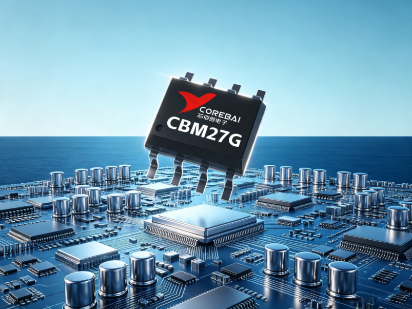
The CBM27G from Corebai is a single-channel precision operational amplifier designed for applications in industrial control, data acquisition, ATE testing equipment, and instrumentation – a single-channel, low-noise, precision bipolar operational amplifier that achieves an input voltage noise density of 3.1nV/√Hz(1 kHz) and a noise level of just 0.1 µVp-p (typical) across the 0.1–10 Hz frequency range when powered by a typical ±15 V supply; it delivers an open-loop gain of 1500 V/mV (typical), while maintaining an GBW product of 8 MHz and a slew rate of 2.8 V/µs. This device supports Pin-to-Pin import substitution; adopting a domestic alternative can shorten delivery timelines and reduce overall material costs.
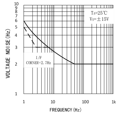
Figure 1: Relationship between voltage noise density and frequency
Architecture and Core Parameters
The CBM27G features a bipolar input stage coupled with a bias current cancellation circuit, which reduces the input bias current to approximately ±15 nA (typical) while maintaining low noise and high gain. The device supports a wide-voltage supply range of ±4 V to ±18 V (i.e., 8 V to 36 V). Its output stage offers excellent load driving capability; with a ±10 V output swing (under a 600 Ω load) combined with low output distortion, it is also suitable for use in professional audio applications.
The following are the key electrical characteristics at 25°C and Vs = ±15 V:
|
parameter |
condition |
representative value |
crest value |
unit |
|
Input offset voltage VOS |
— |
30 |
100 |
µV |
|
失调电压温度漂移 |
— |
0.4 |
1.9 |
µV/℃ |
|
Input bias current IB |
— |
±15 |
±80 |
nA |
|
Input offset current (IOS) |
— |
10 |
75 |
nA |
|
Input Voltage Range (IVR) |
— |
±11.0 |
±12.2 |
V |
|
Common-mode rejection ratio (CMRR) |
VCM=±11V |
110 |
125 |
dB |
|
Open-loop voltage gain (AOL) |
RL≥2kΩ, V0=±10V |
700 |
1500 |
V/mV |
|
Output voltage amplitude |
RL≥600Ω |
±10.0 |
±12.0 |
V |
|
Input voltage noise density (en) |
f=1kHz |
3.1 |
5.0 |
nV/√Hz |
|
0.1–10Hz noise |
— |
0.1 |
0.25 |
µVp-p |
|
Output slew rate (SR) |
RL≥2kΩ |
1.7 |
2.8 |
V/µs |
|
Gain–Bandwidth Product (GBW) |
— |
5 |
8 |
MHz |
|
Power Supply Rejection Ratio (PSRR) |
Vs=±4V~±18V |
95 |
120 |
dB |
|
quiescent dissipationPD |
— |
105 |
175 |
mW |
Key engineering highlights
Low noise level is the primary value proposition of this component. The input voltage noise density is 3.1nV/√Hz (maximum 5.0nV/√Hz) at 1 kHz; within the 0.1–10 Hz frequency range, the noise is as low as 0.1 µVp-p (maximum 0.25 µVp-p), ensuring a clean low-frequency noise profile. When audio or low-frequency sensors are amplified, there is no need for large-value RC filter-based jitter suppression – the noise present in the pre-stage directly determines the overall signal noise floor of the entire system.
High open-loop gain ensures reliable negative feedback accuracy. When combined with 125 dB common-mode rejection and 120 dB power supply rejection, this high open-loop gain significantly reduces measurement errors arising from limited gain, common-mode interference, and power supply ripple. For circuits such as integrators, precision summation circuits, and threshold detection circuits—where high gain is essential to maintain linearity—this high AOL directly translates to lower integration drift and more accurate summation results.
Bias current cancellation enables bipolar circuits to operate at low bias levels. With the help of a bias current cancellation circuit, the input bias current is typically ±15 nA (maximum ±80 nA) – a relatively low value for bipolar op-amps. When combined with an input offset current of typically 10 nA (maximum 75 nA), this ensures that the front-end of most sensors with moderate source impedance will not experience significant offset at the source impedance due to the bias current.
The industrial-grade operating temperature range and wide voltage range provide flexibility in field applications. The power supply covers ±4 V to ±18 V (8 V to 36 V), enabling both dual-power-supply instrumentation and operation under higher single-power-supply conditions; the operating temperature range is −40°C to +85°C, covering typical factory automation and outdoor power acquisition applications – offering superior cost-effectiveness when ultra-low-temperature specifications are not required.
Typical implementation scenarios
This device is designed for several types of low-level signal links:
Process Control and Automation: Pressure transmitters, temperature controllers, PLC/DCS front-end conditioning, and safety barrier isolated amplification – leveraging high gain and low offset to ensure linearity and accuracy; industrial temperature rating compatible with field operating conditions.
Power Electronics and Data Acquisition: Solar inverter current/voltage sampling front-end and power acquisition system; supports a wide voltage range and features 120 dB PSRR for suppression of busbar ripple interference.
ATE and data acquisition: With an 8 MHz bandwidth and a 2.8 V/µs slew rate, it delivers excellent dynamic accuracy in high-speed data acquisition systems.
Professional audio front-end: Microphone and magnetic head preamplifiers, utilizing low noise and low distortion with a ±10 V swing (600 Ω) for clean small-signal amplification.
Weak signal amplification: high-gain amplification of low-level signals in bridge-type sensor and battery testing applications, with minimal low-frequency noise.
What other details should be considered in application design?
Pin 1 (1) and Pin 8 (8) are the TRIM offset zeroing pins; when paired with a 10 kΩ multi-turn potentiometer with the slider connected to V+, the adjustable zeroing range is ±4.0 mV; Pin 5 (5) is NC (floating) – do not route any traces or drill through it.
2. Power supply decoupling: Place a 0.1 µF ceramic capacitor near each of V+ and V− and ground them at a single point; implement independent bypassing for both power supplies to suppress power supply ripple from entering the signal via the limited PSRR path.
3. Output swing and load: The output swing narrows as the load increases; under a ±15 V power supply, a 600 Ω load ensures a stable output of ±10 V, while a 2 kΩ load can yield an output of ±13.3 V. When driving heavy loads, it is advisable to reserve additional voltage margin; if necessary, add a downstream buffer stage.
4. Single-power supply note: The input voltage range (IVR) at ±15 V is approximately ±11–±12.2 V; this range does not include the negative power rail. When using a single power supply, the low-voltage signal referenced to ground must first undergo level shifting; the signal cannot be directly sampled near ground.
The boundary requiring an objective understanding
The CBM27G is a classic precision bipolar operational amplifier, not a rail-to-rail or zero-drift device; it is important to distinguish between these two types.
This is not a rail-to-rail input/output configuration; the dynamic range is limited under a low-voltage single-power-supply setup, and the ground-reference small-signal requires level shifting – therefore, a rail-to-rail CMOS op-amp is more suitable for projects involving a single lithium-ion battery or low-voltage signal acquisition near ground.
The input bias current of ±15 nA may seem relatively low in bipolar circuits, but it is significantly higher than that of JFET/CMOS input devices; however, for high-source-impedance signals—such as those from pH electrodes, photodiodes, or high-impedance bridge sensors—the voltage drop across the source impedance due to the bias current can still introduce a considerable offset; therefore, in such scenarios, JFET/CMOS input operational amplifiers should be given priority when evaluating them.
The maximum offset of 100 µV is relatively low; however, this represents a "low-offset" characteristic rather than "zero-drift" behavior – with a typical temperature drift of 0.4 µV/°C and a maximum of 1.9 µV/°C. For applications requiring extremely precise long-term DC stability, the internal TRIM trimming function can be enabled, or devices featuring a zero-drift architecture can be selected. The 8 MHz bandwidth and 2.8 V/µs slew rate represent a mid-speed performance range; RF or high-speed communication applications are not part of its design objectives.
Why should it be included in the BOM?
For precision analog systems, an excellent operational amplifier is not merely one with higher specifications, but one that achieves a reasonable balance among various performance metrics.
The CBM27G features an optimized balance between input offset, noise, open-loop gain, common-mode rejection, power supply rejection, dynamic performance, and power supply range. For applications such as power utility data acquisition, high-precision data acquisition, automated testing equipment, instrumentation, and professional audio systems, this balanced approach often offers greater practical value than focusing on a single parameter alone.
010-62106066
( Monday to Friday 9:00 - 18:00 )
 704-705, Block D, Building 2, No. 9 Fenghao East Road, Haidian District, Beijing

Wechat Public Account





This app respects and protects the privacy of all users who use the service. In order to provide you with more accurate and personalized services, this app will use and disclose your personal information in accordance with this Privacy Policy. However, this application will treat this information with a high degree of diligence and prudence. Except as otherwise provided in this Privacy Policy, this application will not disclose or provide this information to third parties without your prior permission. This app will update this privacy policy from time to time. By agreeing to this Application Services Use Agreement, you are deemed to have agreed to the entire content of this Privacy Policy. This Privacy Policy is an integral part of this Application Service Agreement.


 Online Store
 A/D Converters (ADC)
 RF Transceiver
 Controller
 Power Management
 Logic gates
 Real-time clocks
 Digital Isolator
 Darlington Transistor
 D/A Converters (DAC)
 Sensors
 Analog Switches Multiplexers
 Interface
 Monitoring Circuit
 Amplifier

 在线商城
在线商城