 Released:2019-04-01 00:00:57
 Views 1851 次
 The radar echo signal operates over a wide frequency band. When sampling the echo signal, according to the Nyquist sampling theorem, the sampling frequency must be greater than or equal to twice the highest frequency of the sampled signal in order to ensure that the sampled signal is not distorted. This places high demands on the accuracy and reliability of the sampling circuit when operating at high frequencies. This article introduces a high-frequency and highly reliable signal acquisition and data formation system, where the maximum frequency of the sampling circuit can reach. Due to the advantages of small size, low power consumption, short development cycle, and flexible configuration of FPGA chips, this system uses FPGA chips as the core to construct signal acquisition and data formation circuits.

1. Foreword
Radar echo signals operate over a very wide frequency band. When sampling these echo signals, according to the Nyquist Sampling Theorem, the sampling frequency must be greater than or equal to twice the highest frequency of the signal being sampled in order to ensure that the sampled signal remains undistorted. This necessitates operation of the sampling circuitry at very high frequencies, imposing stringent requirements on the precision and reliability of the circuitry.
This paper introduces a high-frequency, highly reliable signal acquisition and data formation system, with the capability of achieving a maximum sampling frequency in the circuitry.
Taking advantage of the FPGA chip's compact size, low power consumption, short development cycle, and flexible configuration, this system utilizes an FPGA chip as its core component in constructing the signal acquisition and data formation circuitry.
2. Design Scheme
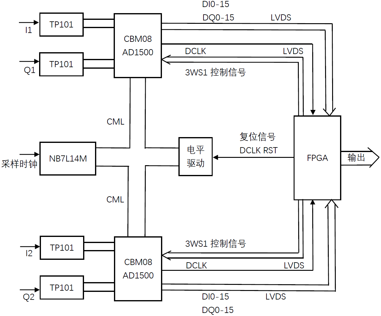
In the signal acquisition and data formation module, two CBM08AD1500QP chips are employed simultaneously to perform sampling of the orthogonal baseband video signals from both the HH and HV radar echo channels. The V5 series FPGA—Vertex5 is utilized to receive the output data from the ADCs, buffer the received data, and undertake the tasks of data interfacing and formatting. The system block diagram is depicted in Figure 1.

Figure 1. Overall design block diagram of the data acquisition system
Two CBM08AD1500QP devices sample the baseband video signals of the two positive traffic channels in the radar echo. The sampled data is output using the LVDS voltage level standard, with each ADC producing a 32-bit digital signal in parallel format. Both sets of signals are received by a single Vertex5 FPGA.
The FPGA also implements interface conversion and control functions. It features an external auxiliary data interface that receives control commands from the main controller for the signal acquisition and data formation module. Additionally, it houses two 32-bit wide data recording interfaces, which打包 the sampled data from both ADCs along with the auxiliary data into frames, subsequently sending these frames through either the dual data recording interfaces or the RockeIO interface to the data recorder.
The ADCs for the two positive traffic channels have stringent requirements for inter-channel synchronization during operation. In this design scheme, a high-speed clock driver NB7L14M is employed to drive the sampling clock, ensuring phase consistency in the sampling clock signals reaching both ADCs. This design incorporates self-test functionality, allowing it to transmit self-test results to the main controller via telemetry signals. The system is designed to operate at a maximum frequency of 1.5 GHz.
3. Peripheral Circuit Design of AD
The signal acquisition and data formation module utilizes the CBM08AD1500QP analog-to-digital conversion (ADC) chip for its tasks. This chip is a dual-channel, low-power CMOS analog-to-digital converter (ADC) introduced by National Semiconductor Corporation. It boasts a sampling frequency of 1.7 GSPS, an 8-bit resolution, and offers the option of either SDR or DDR output clocking. Operating in Dual Edge Sampling (DES) mode, it can sample at a rate of 3 GSPS using a single analog input channel. In this system, both input channels are utilized to perform sampling at a rate of 1.5 GSPS.
(1)Analog Input
Each CBM08AD1500QP chip features two analog input channels, designated as VINI and VINQ, both of which require differential input signals. The upstream data source provided in this setup, however, supplies single-ended signals. To accommodate the ADC's differential input requirement, a transformer is employed to convert the single-ended signals into differential form. In this design, the single-ended analog input signals are processed by a radio frequency (RF) transformer, model TP-101, which subsequently feeds the converted differential signals into the analog input terminals of the ADC.
(2)Clock Input
The ADCOSDl500 chip possesses a pair of differential clock input pins, CLK+ and CLK-, operating in an LVDS (Low Voltage Differential Signaling) standard. These inputs are designed for AC-coupled differential signals. The incoming clock signal is capacitively coupled to the ADC's clock input via a 4.7 nF capacitor. According to the design specifications, the sampling clocks for the two ADCs must be tightly synchronized to ensure their amplitude and phase consistency requirements are met.
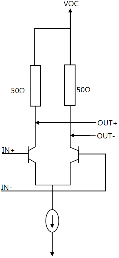
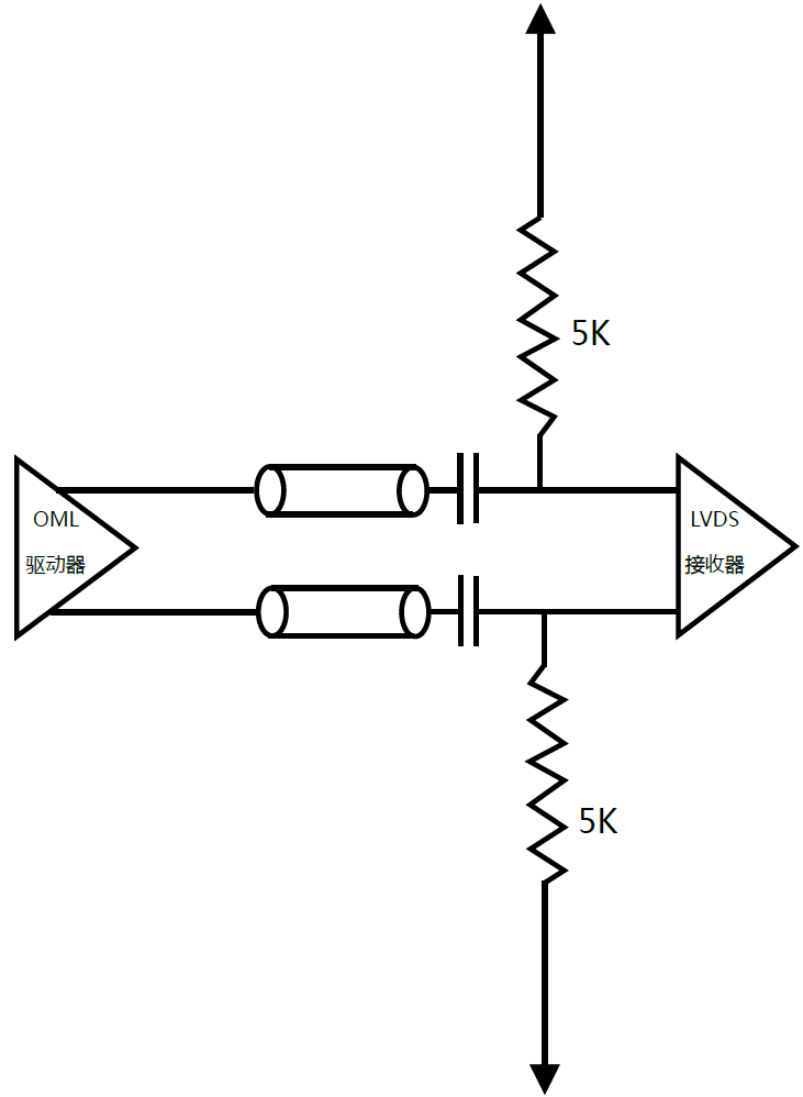
In the driver design, a high-speed 1:4 clock distribution chip, the NB7L14M from on semiconductor, is employed to accomplish this synchronization. This device accepts input signal levels in LVPECL, CML, LVDS, LVTTL, and LVCMOS formats, and its outputs are standardized as CML level signals, which are then AC-coupled to the clock inputs of the ADCs. The output structure of the CML interface is depicted in the following figure. A typical CML interface output circuit takes the form of a differential pair, with a constant current source of typically 16 mA from the emitter to ground in each branch. Assuming a CML output load consisting of a 50 Ω pull-up resistor, the single-ended CML output signal swing is VCC - (Vcc - 0.4V). Under these conditions, the differential output signal swing amounts to 800 mV.
The AC-coupling circuitry for transitioning from CML to LVDS is shown in the following figure.

Figure 2. CML Output structure

Figure 3. CML to LVDS in AC coupling circuit diagram
(3)Reset signal
According to design specifications, the reset signals for both ADCs must also adhere to stringent timing synchronization requirements. After generation by the FPGA, the reset signals produced by the FPGA are separately fed into the DCLK_RST terminals of each of the two AD chips, thereby effectuating synchronous resets on both ADCs.
(4)Control signal
This AD converter offers two types of control interfaces: one via level control and the other through complex control via the SPI port. The latter enables utilization of all functionalities of this AD model in an extended mode.
4. The data interface circuit between the AD (Analog-to-Digital Converter) and FPGA (Field-Programmable Gate Array)
The single-chip ADC has an output word width of 32 bits. Its 32-bit parallel output data is received by a single Vertex-5 FPGA, which performs parallel-to-serial conversion and buffers high-speed sampled data for deceleration.
The Vertex-5 is the fifth-generation product in Xilinx's Vertex series. It features 24 RocketIO transceivers operating within a range of 100 Mbps to 3.2 Gbps, incorporating an on-chip PCI Express module and a triple-mode Ethernet Media Access Controller (MAC) module. The Vertex-5 supports interfaces such as LVDS and LVPECL, among others.
Each ADC output signal comprises 32-bit sampled output data, a single data synchronization clock (DCLK), a sampling overflow signal (OR), and an indication signal for ongoing self-calibration (CalRun). All signals except CalRun have LVDS output levels.

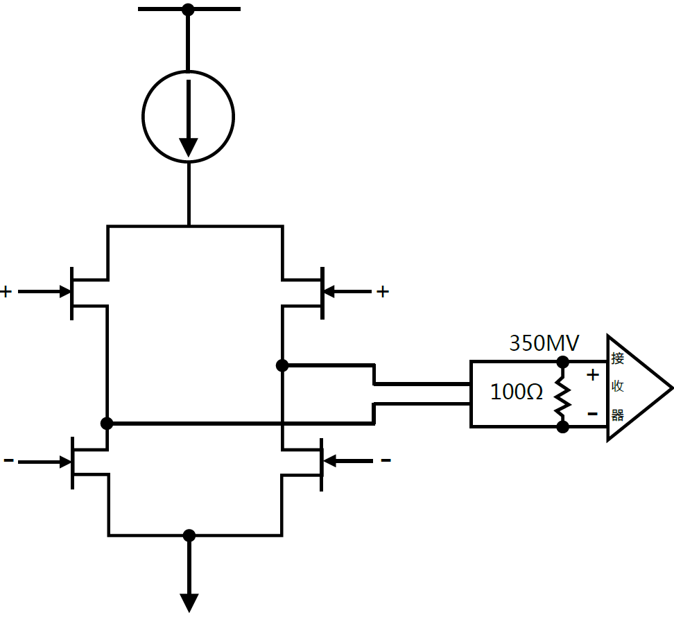
Figure 4. LVDS operational principle
LVDS (Low Voltage Differential Signaling) is a standard for small amplitude differential signaling. The typical working principle of LVDS is shown in Figure 1, with the most basic LVDS devices being the LVDS driver and receiver. The LVDS driver consists of a current source driving the differential lines, typically with a current of 3.5 mA. The LVDS receiver has a very high input resistance, so the majority of the current output by the driver flows through a matched resistor of 100 Ohms, generating approximately 350 mV at the receiver's input. When the driver toggles, it reverses the direction of the current flowing through the resistor, thus producing valid logic 1 and logic 0 states. LVDS exhibits excellent characteristics such as high speed, ultra-low power consumption, low noise, and low cost.
In board-level design, attention should be given to the following points regarding LVDS:
1. Maintain equal spacing and length of differential lines: This helps prevent phase differences between signals that can cause radiation. The distance between the two differential lines should be as close as possible to enhance the common-mode rejection capability of the receiver.
2. Ensure continuous return paths for LVDS signal lines on the PCB: Avoid crossing splits, as transmission lines spanning the split will experience impedance discontinuity due to the absence or non-continuity of the reference plane.
3. Minimize the number of vias: Given the current-carrying requirements are met, smaller via diameters result in smaller capacitive and inductive effects.
4. Avoid 90-degree corner routing that causes impedance discontinuity: Use arcs or 135-degree angled lines instead.
5. Implement termination resistors for optimal matching of the differential lines: These resistors serve to absorb reflected load signals, with the differential impedance generally controlled within the range of 85 to 115 Ohms.
5.Design of RocketlO Transceiver Interface for FPGA
The RocketIO transceivers in the Vertex5 employ fourth-generation gigabit-level transceiver technology, operating at speeds ranging from 100 Mbps to 3.75 Gbps. At the 3.75 Gbps rate, each channel consumes less than 100 mW of power, representing the industry's lowest power consumption. Advanced TX/RX equalization techniques are employed, facilitating adjustments on certain channels to ensure reliable operation. Integrated PRBS transmitters and checkers simplify characterization and debugging.
This system utilizes the RocketIO transceivers in the Vertex5 to implement serial output of sampled data. To guarantee the reliable functioning of the RocketIO transceivers, hardware circuit design must adhere to certain requirements, considering the following aspects:
(1)Reference clock design:
The RocketIO transceiver requires a high-precision differential clock. This system employs the Epson EG-2121CA differential output (LVDS) crystal oscillator recommended by Xilinx, which offers a frequency range of 53.125 MHz to 700 MHz and exhibits low jitter (RMS Period: 3 ps; Peak to Peak: 25 ps). This oscillator satisfies the performance requirements for the reference clock in the RocketIO module within the design.
(2)Power supply design:
The power pins of RocketlO transceivers are sensitive to the impact of noise, so specialized power supply is needed to isolate the influence of peripheral noise sources. Each power supply pin has its own LC filtering network.
(3)PCB design:
During routing, particular attention should be paid to the fact that, due to the high frequency of the transmitted signals, differential signal lines must be matched in length as closely as possible. Severe mismatches can result in significant jitter and unpredictable timing issues.
6.Conclusion
This paper presents a detailed design of an acquisition system based on the high-speed conversion chip CBM08AD1500QP and a top-end FPGA Vertex-5, achieving a speed of 1.5 Gbps suitable for modern broadband communications. The system is characterized by its compact size, low power consumption, and flexible, user-friendly operation. Notably, the integration of the RocketIO transceiver significantly enhances the speed and reliability of signal transmission between chips, contributing greatly to the overall performance improvement of the radar system.
Article Innovations:
1. The signal sampling and data formation system utilizing the Vertex5 FPGA and the CBM08AD1500QP implements serial output of sampled data through the adoption of fourth-generation gigabit-level transceiver technology in the RocketIO transceiver.
Introduction of CBM08AD1500QP by ChipBest Microelectronics: The CBM08AD1500QP is fully compatible with the ADC08D1500.
010-62106066
( Monday to Friday 9:00 - 18:00 )
 704-705, Block D, Building 2, No. 9 Fenghao East Road, Haidian District, Beijing

Wechat Public Account