

 Released:2026-08-05 17:50:40
 Views 403 次
 消费电子里的音频对接系统——蓝牙音箱、智能音箱、车载音响、会议终端——工程师最头疼的往往不是"能不能出声",而是"出声干不干净、失真大不大"。模拟音频链路一旦被噪声、失真、电源纹波污染,后期软件降噪也救不回来;而供电又是另一道坎:开关电源效率高,但纹波会直接进入音频地;线性稳压输出干净,压降与散热却是主要约束。

In consumer electronics, audio interfacing systems—such as Bluetooth speakers, smart speakers, car audio systems, and conference terminals—often present engineers with challenges that go beyond simply "whether sound can be produced"; rather, the real issues are "whether the output sound is clean or whether there is significant distortion." Once an analog audio link is contaminated by noise, distortion, or power ripple, subsequent software-based noise cancellation cannot remedy the problem; furthermore, power supply design poses another major hurdle: while switching power supplies offer high efficiency, their ripple directly couples into the audio ground; conversely, linear regulators provide a cleaner output but face primary constraints in terms of voltage drop and heat dissipation.
Most of the solutions to these challenges lie in the selection of front-end components. Corebai provides a complete audio analog solution suite: the preamplifier family includes the high-performance CBM8655 model and the general-purpose CBM8605 model, designed respectively for high-fidelity applications and mass-produced general audio scenarios; the low-noise 3.3V power supply required for the audio circuit is provided by the CBM1117 linear regulator.
Signal chain: from AUXIN to speaker
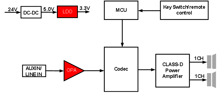
Figure: Block diagram of the audio interface system's signal chain and power supply chain
External audio signals entering the card via the AUXIN or LINE IN inputs first pass through a first-stage operational amplifier for conditioning, then proceed to the codec for encoding and decoding, and finally are driven by the CLASS-D amplifier to the speakers. This pre-amplification stage directly determines the overall system's background noise level and fidelity.
· High-fidelity audio scenario selection → CBM8655. It reduces the noise density to 2.7nV/√Hz (10 kHz), representing one of the lowest levels among precision CMOS op-amps in its class; a THD+N of 0.0007% indicates minimal harmonic distortion even at high signal levels. Combined with a gain-bandwidth product of 28 MHz and an slew rate of 11 V/μs, this op-amp can maintain clean waveforms in AC applications ranging from microphones to mixing consoles. It also outputs ±220 mA (with a 5V supply), providing ample headroom when the pre-stage buffers the post-stage. The rail-to-rail input/output capability allows a single 5V system to fully utilize its output swing. Operating within a temperature range of −40°C to +125°C, it is suitable for automotive audio or outdoor applications. In noise-sensitive scenarios such as microphone pre-amplification and mixing consoles, system-level noise can easily mask details; the low noise and low distortion characteristics of the CBM8655, coupled with its high output current, perfectly meet these requirements.
· For high cost-effectiveness and versatile audio channels, choose the CBM8605. It features low noise 12nV/√Hz, a gain bandwidth of 8.7 MHz, a very low bias current of just 1 pA, rail-to-rail operation, and operates on a single power supply ranging from 2.7 V to 5.5 V. Its performance meets general audio conditioning requirements, while its BOM cost is even lower; the extremely low bias current of 1 pA, when paired with a high-impedance input for a piezoelectric or silicon microphone preamplifier interface, ensures no additional offset is introduced at the source impedance.
Both components operate on a single power supply and feature rail-to-rail performance, eliminating the need for additional level conversion when directly interfacing with an MCU or codec. Only one preamplifier should be used per audio channel; for symmetrical channels such as left and right channels, it is recommended to use identical models to ensure channel consistency and avoid any potential sound quality discrepancies between the left and right channels resulting from mixing different amplifier levels.
Power supply chain: 24V input, 3.3V clean output
In this design, the 24V bus first undergoes DC-DC conversion to 5V, then is regulated by the CBM1117 to 3.3V to power the MCU and analog module. Note that the absolute maximum input voltage for the CBM1117 is 15V; the output from the DC-DC stage must be kept below 15V before being connected to the circuit. Why is it not advisable to directly use the DC-DC output at the 5V to 3.3V stage? If the switching ripple from the DC-DC converter were introduced directly into the analog front-end, it would be amplified by the operational amplifier into audible noise. For LDOs such as the CBM1117, the ripple suppression ratio at 120Hz is typically 60dB, which effectively attenuates the ripple to one-thousandth of its original level, thereby significantly reducing the background noise.
The CBM1117 has an output current of 0.8 A and supports multiple fixed voltage levels: 1.2 V, 1.5 V, 1.8 V, 2.5 V, 3.3 V, and 5 V; it also supports adjustment via an external resistor to a range of 1.25 V–13.8 V. The output voltage accuracy is ±2%, and the device features current limiting and overheat protection. In a 24 V → 5 V → 3.3 V circuit configuration—using a light-load scenario where the input is 5 V and the output is 3.3 V (resulting in a voltage drop of approximately 1.7 V), with a load of 200 mA—the power consumption is approximately 0.34 W, and the temperature rise for the SOT-223 package (θJA ≈ 150°C/W) is approximately 50°C, which is controllable. However, when operating at the maximum output current of 0.8 A, the power consumption increases to approximately 1.36 W, causing the temperature rise of the SOT-223 package to exceed 200°C—far surpassing the junction temperature limit; under these conditions, it is necessary to switch to the TO-252 package (θJA ≈ 80°C/W) and implement extensive copper pad layout for heat dissipation; therefore, the SOT-223 package is only suitable for light-load scenarios with currents ≤ 300 mA.
Key Engineering Points and Design Constraints
· Power decoupling and ground separation: Place the op-amp's power pins near the circuit, with a 0.1µF + 10µF bypass capacitor; connect the analog ground and digital ground at a single point; it is recommended to place this common ground connection near the ground terminal of the LDO output capacitor to prevent digital return current noise from coupling into the analog power supply. For the CBM1117, a tantalum capacitor with a capacitance of 10µF or higher is recommended on the output side to stabilize transient responses.
· The swing range varies with the load. The rail-to-rail output exhibits a voltage drop depending on the load current: according to technical specifications, at a 1 mA load, the output voltage deviates from the power supply rail by only approximately 20–40 mV; at 10 mA, the high-side voltage drops to approximately 210–300 mV. When designing a full-range circuit, it is essential to incorporate a margin based on the actual load rather than relying on ideal rail-to-rail calculations.
· Temperature boundary: All three components have a nominal operating temperature range of −40°C to +125°C; however, the continuous current capability of the LDO is constrained by its package's thermal dissipation capacity, meaning that in high-current applications, the device must be derated based on its thermal resistance.
· Separation of digital and analog power supplies. In this solution, the MCU and the analog front-end share the 3.3 V supply from the CBM1117; for noise-sensitive audio channels, it is recommended to route the MCU's digital power supply through a separate DC-DC converter, while the analog audio section is powered independently by the CBM1117, thereby further reducing digital noise crosstalk.
· Accuracy limits: For the CBM8655, the maximum offset voltage is 250 µV; for the CBM8605, the maximum offset voltage across the full common-mode input range is 300 µV (with a maximum of 65 µV only under the narrow operating conditions where VS = 3.5 V and VCM = 3 V). Both devices fall into the "precision" category rather than the "zero-drift" category; therefore, these devices should be used with caution in pure DC precision measurement applications.
Quick Reference Guide to Core Components of the Solution
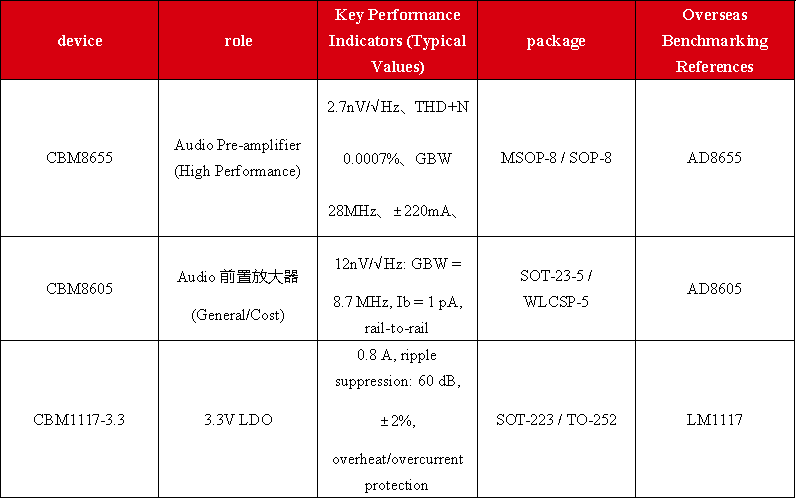
These three devices are pin-compatible with the AD8655, AD8605, and LM1117, supporting direct pin-to-pin replacement.
010-62106066
( Monday to Friday 9:00 - 18:00 )
 704-705, Block D, Building 2, No. 9 Fenghao East Road, Haidian District, Beijing

Wechat Public Account





This app respects and protects the privacy of all users who use the service. In order to provide you with more accurate and personalized services, this app will use and disclose your personal information in accordance with this Privacy Policy. However, this application will treat this information with a high degree of diligence and prudence. Except as otherwise provided in this Privacy Policy, this application will not disclose or provide this information to third parties without your prior permission. This app will update this privacy policy from time to time. By agreeing to this Application Services Use Agreement, you are deemed to have agreed to the entire content of this Privacy Policy. This Privacy Policy is an integral part of this Application Service Agreement.


 Online Store
 A/D Converters (ADC)
 RF Transceiver
 Controller
 Power Management
 Logic gates
 Real-time clocks
 Digital Isolator
 Darlington Transistor
 D/A Converters (DAC)
 Sensors
 Analog Switches Multiplexers
 Interface
 Monitoring Circuit
 Amplifier

 在线商城
在线商城