

 Released:2026-07-31 10:20:07
 Views 586 次
 医疗成像前端、通信接收机中频采样、便携式工业仪表、低功耗数字示波器,四大赛道均存在统一采集需求:14bit 分辨率、50MSPS 高速采样,同时对芯片体积、整机功耗、供应链稳定性提出硬性约束。在国产化加速的背景下,工程师关注的已不仅是参数达标,而是真正具备量产能力、供货稳定且批量一致性良好的国产高速 ADC。

From medical imaging front-end systems and communication receiver intermediate-frequency sampling modules to portable industrial instruments and low-power digital oscilloscopes, all four major application domains share unified acquisition requirements: 14-bit resolution, 50 MSPS high-speed sampling rates, along with stringent constraints on chip size, overall power consumption, and supply chain reliability. Amid the accelerated pace of domestic technological development, engineers now focus not merely on meeting technical specifications but on achieving domestically produced high-speed ADCs that possess genuine mass-production capability, stable supply reliability, and excellent batch consistency. When components are integrated into product bills of materials (BOM), their ability to directly replace existing boards and whether their performance meets mass-production demands often proves more decisive than mere technical parameters.
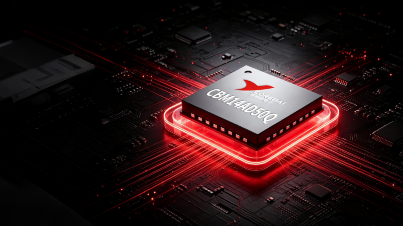
To address the critical demand for domestic industry solutions, Corebai has developed its proprietary solution—the ADC CBM14AD50Q, featuring a standard 14-bit architecture with 50 MSPS performance. Its pin configuration and electrical specifications align with the industry's mainstream general standards for high-speed ADCs of similar specifications. Existing mature boards can be directly upgraded using this component without modification or reconfiguration, enabling rapid achievement of domestic substitution.
I. Chip Hardware Architecture and Packaging Specifications
The chip employs a mature CMOS process-based monolithic integrated pipeline architecture, featuring integrated components such as a sampling-and-holding amplifier, multi-stage ADC conversion cores, high-precision reference source, clock jitter stabilization circuit, and hardware mode control logic. This high integration significantly reduces the number of peripheral devices and simplifies the overall BOM design.
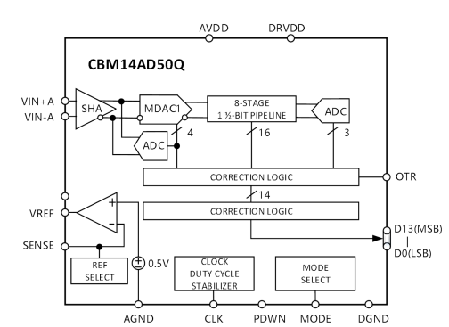
The package employs the industry-standard QFN32 configuration with dimensions of 5.0 mm × 5.0 mm × 0.75 mm, featuring large exposed heat dissipation pads on the bottom (specified for connection to analog ground), balancing compact size with effective thermal performance for use in space-constrained portable devices. It provides a 14-bit parallel CMOS level output (D0–D13, with D13 as the most significant bit/MSB) that directly interfaces with FPGA/DSP parallel buses, eliminating the need for additional level conversion chips.
The pin layout and electrical parameters comply with industry-standard specifications, eliminating the need for redesign during domestic upgrades of existing equipment and enabling seamless mass production transitions.
II. To what level does the product truly reach?
The following key parameters were measured under the following conditions: simulated power supply of 3 V, digital power supply of 2.5 V, 50 MHz sampling rate, differential input of 2 VPP, and operating temperature range of −40 to 85 °C:

Core Performance Analysis:
The SNR typically reaches 67.8 dB, and the SFDR typically reaches 82 dB, covering the dynamic range of intermediate frequency sampling and imaging front-end stages.
The DNL standard has a tolerance of ±0.9 LSB, ensuring monotonic code values and no bit loss. The INL standard has a tolerance of ±3.4 LSB, meeting requirements for general industrial, medical, and communication equipment applications.
The typical aperture delay is 1.4 ns, with output delays ranging from 2.0 to 6.0 ns; the pipeline delay remains fixed at 7 clock cycles. The timing budget calculation is straightforward, and multi-channel waveform synchronization along with timing alignment significantly reduce development complexity.
Supports dual independent power supplies: analog (3.0–3.3 V) and digital (2.5–3.3 V), with digital IO operating at standard CMOS voltage levels. Features a built-in high-precision reference voltage range of 0.965–1.035 V, eliminating the need for external precision reference circuits.
III. Two Flexible Configurations Engineers Will Appreciate
The CBM14AD50Q offers considerable flexibility in terms of usage:
The reference voltage offers three configuration options: direct use of the internal fixed 1 V reference (corresponding to a 1 VPP input range); selection of an external reference; or configuration of a programmable reference via the SENSE pin, utilizing an external resistor ratio to extend the input range to 2 VPP. Both single-ended and differential inputs are supported—differential inputs can be driven by an amplifier or implemented with transformer coupling, providing significant flexibility for front-end circuit design.
The output data format is selected via the MODE pin: binary complement code or binary shift code; this same pin also controls the enable status of the internal clock stabilization circuit. When the power-saving pin PDWN is pulled high, the entire chip enters a low-power state with consumption reduced to 15 mW and all outputs remain high-impedance; pulling it low (default state) restores normal sampling operation. For portable or power-sensitive devices that operate in sleep mode most of the time with only occasional sampling, the 15 mW standby power consumption proves highly practical.
IV. Typical Application Scenarios
1. High-end medical imaging equipment
Featuring 14-bit high precision and an 82 dB high SFDR dynamic range, with differential input suppression for common-mode interference, it accurately reproduces subtle human signal grayscale details and is suitable for use in ultrasound and imaging acquisition systems.
2. Sampling of intermediate-frequency signals in a communication receiver
Featuring 50 MSPS full-speed sampling with an integrated clock stabilization circuit that suppresses clock jitter, it delivers excellent FFT noise floor performance for high-and low-frequency intermediate signals, making it ideal for RF down-conversion digital links.
3. Portable Industrial Instrument
5×5 mm compact QFN package with hardware-powered power-saving standby mode, reducing average power consumption for battery-powered devices—ideal for handheld data collectors and portable testing equipment.
4. Low-power digital oscilloscope
The 14-bit parallel CMOS output can directly connect to the FPGA buffer waveform, featuring a fixed 7-cycle pipeline delay that simplifies waveform timing synchronization and streamlines the design of the oscilloscope's front-end sampling circuit.
5、Value of Device Selection
Meeting parameter specifications is only the foundation; standardizing hardware design and welding processes is essential to ensure both overall yield rates and long-term stability of the equipment.
The CBM14AD50Q integrates all essential modules required for this sampling rate range—including sample-and-hold, ADC core, reference voltage, clock stabilization circuit, and mode selection—into a single 5×5 mm QFN-32 package, offering industry-standard parallel CMOS interfaces while simplifying both front-end driver integration and back-end FPGA connectivity.
With a typical SNR of 67.8 dB and SFDR of 82 dB, coupled with a DNL of ±0.9 LSB, the system ensures monotonic code values without bit loss, covering typical applications such as medical imaging, intermediate-frequency sampling, portable instruments, and oscilloscopes.
The more practical advantage lies in the fact that, as a domestically developed component, it offers predictable supply and delivery timelines, with pin compatibility matching mainstream solutions in its class, eliminating the need to trade performance for supply chain considerations when evaluating alternatives.
010-62106066
( Monday to Friday 9:00 - 18:00 )
 704-705, Block D, Building 2, No. 9 Fenghao East Road, Haidian District, Beijing

Wechat Public Account





This app respects and protects the privacy of all users who use the service. In order to provide you with more accurate and personalized services, this app will use and disclose your personal information in accordance with this Privacy Policy. However, this application will treat this information with a high degree of diligence and prudence. Except as otherwise provided in this Privacy Policy, this application will not disclose or provide this information to third parties without your prior permission. This app will update this privacy policy from time to time. By agreeing to this Application Services Use Agreement, you are deemed to have agreed to the entire content of this Privacy Policy. This Privacy Policy is an integral part of this Application Service Agreement.


 Online Store
 A/D Converters (ADC)
 RF Transceiver
 Controller
 Power Management
 Logic gates
 Real-time clocks
 Digital Isolator
 Darlington Transistor
 D/A Converters (DAC)
 Sensors
 Analog Switches Multiplexers
 Interface
 Monitoring Circuit
 Amplifier

 在线商城
在线商城