

 Released:2026-08-12 11:13:21
 Views 371 次
 核心亮点抢先看 ▶ 12 位、500MSPS 流水线 ADC,实测 SFDR 达 79.23 dBFS,宽带动态余量充足 ▶ 1.8V 单电源、LVDS 输出、SPI 可控,片内集成 SHA 与基准,外置元件少 ▶ 引脚兼容 AD9434BCPZ-500,国产化替换无需改动板级布局

Key Highlights: Preview
▶ A 12-bit, 500 MSPS流水线ADC achieves a measured SFDR of 79.23 dBFS, with ample wideband dynamic range.
▶ 1.8 V single supply, LVDS output, SPI-controlled, features integrated SHA and reference voltage source, with minimal external components required
▶ The AD9434BCPZ-500 is pin-compatible; localized substitution requires no modifications to the board-level layout.
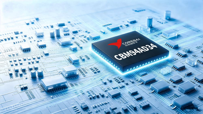
Q1: What is the CBM94AD34-500 component? Is it suitable for my project?
This is a 12-bit resolution, 500 MSPS maximum sampling rate pipeline ADC fabricated using the SiGe BiCMOS process and housed in a QFN-56 package. If your project involves applications requiring high-speed, high-dynamic-range acquisition—such as wireless broadband reception, communication test and measurement, radar/satellite echo acquisition, or power amplifier linearization (DPD)—this component is perfectly suited for such scenarios.
Selection Guidelines: For acquisition front-end systems where "high speed + wide bandwidth for dynamic performance" is the primary requirement, these options should be given priority; however, if the project primarily involves high-precision DC measurement, the system's static accuracy may not be its strongest feature, and a separate evaluation is warranted.
Q2: What are its specific resolution and sampling rate? What is the maximum sampling rate it can support?
The resolution is 12 bits, with a maximum sampling rate of 500 MSPS and a minimum conversion rate as low as 50 MSPS; the data delay does not exceed 10 ns.
Design Tip: The 500 MSPS configuration paired with a 12-bit converter is suitable for direct sampling at intermediate frequencies (ranging from tens to hundreds of megahertz); when operating in the second or third Nyquist zones for undersampling, it must be combined with a transformer-coupled input to maintain the SNR.
Q3: Which typical applications will utilize it?
Typical applications include: wireless/broadband communication receivers, communication test and measurement equipment, radar and satellite subsystems, and power amplifier linearization. A common characteristic of these scenarios is that the front-end signals operate at high frequencies and are highly sensitive to both SFDR and ENOB.
Adapter Note: For receive links involving multiple carriers or adjacent channel interference, prioritize verifying whether their measured SFDR (approximately 79 dBFS at 30.3 MHz) meets the system margin requirements.
Q4: Is component replacement easy? Is it pin-compatible with imported solutions?
The CBM94AD34-500 is pin-compatible with the imported AD9434BCPZ-500, and both devices share the same QFN-56 package (8 × 8 × 0.75 mm). For designs based on this imported component, the device can typically be directly substituted in evaluations without requiring a board-level redesign.
Selection Guidelines: This product is recommended as the preferred domestic alternative for imported ADCs in the same class with a 500 MSPS sampling rate; prior to replacement, it is still advisable to verify the board-level details regarding power decoupling and the clock path, and to conduct comparative tests using the original manufacturer's evaluation board.
Q5: How do I connect a digital interface? Is it compatible with an FPGA?
The digital output complies with the ANSI-644 LVDS standard and provides a data clock output (DCO), facilitating direct connection to an LVDS receiver on an FPGA or custom ASIC. The output data format supports binary signed magnitude, Gray code, and offset binary, with switching via SPI; the default output format is offset binary.
Design Tip: It is recommended to use a single-point point-to-point network with a 100 Ω termination resistor; the termination should be placed as close as possible to the receiver. Differential traces should be of equal length and should avoid excessive length (it is recommended not to exceed 24 inches), as otherwise, timing errors may occur.
Q6: Which external function modules are required?
The IC integrates a sampling-and-hold amplifier (SHA) and a reference voltage source, eliminating the need for external components for these two sections. The external components primarily required are: a low-jitter differential clock, a power bypass, and a front-end differential input driver (either a transformer or a differential amplifier). The VREF pin supports switching between internal and external reference modes.
Design Tip: The reference voltage can operate using the default in-package configuration; however, if the system has specific requirements regarding reference temperature drift, the external reference mode can be enabled via SPI—though this will increase board-level complexity and is not recommended unless absolutely necessary.
Q7: What are the actual dynamic performance specifications? What are the values for SNR and SFDR?
At a 500 MSPS clock frequency and a 30.3 MHz input: SNR ≥ 63 dBFS, SINAD ≥ 62 dBFS, ENOB ≥ 10.0 bit, and SFDR ≥ 65 dBFS; under actual measurement conditions, the SFDR can reach 79.23 dBFS, with harmonic rejection exceeding 78 dBFS. When the input frequency is increased to 450.3 MHz, the SNR remains ≥ 61 dBFS and the ENOB remains ≥ 9.5 bit.
Selection Guidelines: For broadband communication and intermediate frequency undersampling applications, you may confidently perform a link budget calculation using measured SFDR values in the 79 dBFS range; however, this option is not recommended as the primary choice for scenarios with high static accuracy requirements.
Q8: Can the input range be adjusted? How is the preamplifier driven?
The analog input range can be adjusted between 1.18 Vp-p and 1.6 Vp-p. Baseband applications can be driven by a differential amplifier; for intermediate frequency undersampling (above 70–100 MHz), differential balun coupling is recommended, with particular attention paid to transformer core saturation and signal power.
Design tip: Once the high-frequency Nyquist region is entered, the noise levels of most amplifiers will no longer meet the SNR requirements; transformer coupling is therefore a more stable option; parallel capacitors should be adjusted according to the input frequency and source impedance, and may be removed if necessary.
Q9: What are the requirements for the clock signal? How significant is the impact of jitter?
The device requires a differential clock (CLK⁺/CLK⁻) with an internal bias of approximately 0.9 V; it supports either transformer AC coupling or differential PECL AC coupling inputs; when using DC coupling, the common-mode voltage must be maintained at 0.9 V. The typical aperture jitter of the device is 80 fs RMS.
Design Tip: Clock jitter directly determines the high-frequency SNR; therefore, a low-jitter clock source (such as a low-noise clock driver) should be used, with transformer coupling prioritized to limit the signal swing and preserve fast edges.
Q10: What are the hard constraints of the drawing board?
Key points: ① The circuit board should feature a complete and clean ground plane; it is recommended to use a multilayer board with separation between digital and analog grounds; ② AVDD, DRVDD, and VCM should be connected to high-quality ceramic bypass capacitors, positioned as close as possible to the pins, with short and wide traces; ③ Differential inputs should be placed as close together as possible and aligned parallel; input traces should be kept as short as possible to minimize parasitic effects; ④ Bare pads at the bottom should be soldered to the large-area ground plane of the PCB, balancing heat dissipation with ground connection.
Design Tip: Avoid routing digital traces directly beneath the ADC; improper grounding of the ground plane can directly degrade dynamic performance, making grounding at the heat-sink pads a mandatory requirement rather than an optional step.
Q11: How is multi-panel synchronization handled?
The CBM94AD34-500 does not natively incorporate multi-chip synchronous logic; synchronization in multi-chip systems relies on all chips sharing a low-jitter differential clock, and ensures time alignment at the receiver end by aligning the DCO with the data format.
Precautions: For multi-channel acquisition systems, the clock source should be unified, and the trace lengths for each channel should be kept equal; the synchronization accuracy is primarily determined by the clock distribution network rather than by the individual components themselves.
Q12: How should I choose the temperature rating and packaging?
Operating temperature range: −40 °C to 85 °C (Industrial grade). Available order models include the CBM94AD34-500 and CBM94AD34-370 (370 MSPS version), both offering two speed grades; all units are packaged in QFN-56 packages with ribbon packaging (260 chips per roll).
Procurement Note: For 500MSPS and 370MSPS models, simply select the appropriate model based on your actual sampling rate requirements; both models share the same package type and can be used in a shared board-level design; their temperature ratings already cover industrial field applications, eliminating the need for additional screening.
Q13: Can I request samples? What types of supporting documentation are required?
You may request sample boards and obtain technical documentation and evaluation support through official manufacturer channels. During the design phase, it is recommended to use an evaluation board to verify dynamic performance and confirm replacement compatibility.
Adapter Tip: For the first domestic substitution, it is recommended to follow a two-step approach— "evaluation board comparison test → board-level small-batch verification" —to mitigate import risks.
Q14: How does power consumption and battery-saving mode work?
Operating power consumption ≤ 900 mW, standby mode ≤ 60 mW, sleep mode ≤ 12 mW. The standby and sleep modes are controlled by the PWDN pin and the SPI configuration.
Design Tip: For intermittent operation or battery-powered devices, enable standby/sleep mode to manage the thermal budget; upon waking, the clock and data timing must be re-established, with sufficient stabilization time reserved in the software.
Selection Summary
The CBM94AD34-500 is designed for high-speed acquisition scenarios such as wireless broadband, test measurement, radar, and DPD, featuring a 12-bit resolution, 500 MSPS sampling rate, and an SFDR of approximately 79 dBFS based on measured values; its core value lies in its pin compatibility with imported counterparts in the same class, enabling localized substitution without requiring board modifications. When selecting this device, dynamic performance and ease of replacement should be the primary criteria for evaluation, while static accuracy and input amplitude (≤1.5 Vp-p) should be considered as critical boundary parameters. For acquisition front-end applications that prioritize "high speed + wide dynamic range + low replacement cost," this component is highly recommended for inclusion in the BOM.
010-62106066
( Monday to Friday 9:00 - 18:00 )
 704-705, Block D, Building 2, No. 9 Fenghao East Road, Haidian District, Beijing

Wechat Public Account





This app respects and protects the privacy of all users who use the service. In order to provide you with more accurate and personalized services, this app will use and disclose your personal information in accordance with this Privacy Policy. However, this application will treat this information with a high degree of diligence and prudence. Except as otherwise provided in this Privacy Policy, this application will not disclose or provide this information to third parties without your prior permission. This app will update this privacy policy from time to time. By agreeing to this Application Services Use Agreement, you are deemed to have agreed to the entire content of this Privacy Policy. This Privacy Policy is an integral part of this Application Service Agreement.


 Online Store
 A/D Converters (ADC)
 RF Transceiver
 Controller
 Power Management
 Logic gates
 Real-time clocks
 Digital Isolator
 Darlington Transistor
 D/A Converters (DAC)
 Sensors
 Analog Switches Multiplexers
 Interface
 Monitoring Circuit
 Amplifier

 在线商城
在线商城