

 Released:2026-07-09 15:24:50
 Views 687 次
 核心亮点抢先看 ·Pin-to-pin兼容AD9779BSVZ:软硬件高度适配,无需改板改驱动,替代迁移成本低 ·1GSPS16位双通道:通信级动态性能,80MHz中频下单载波WCDMA ACLR典型值80dBc ·高集成单芯片方案:内置插值/调制/PLL/辅助DAC,精简射频发射前端架构 ·工业级低功耗设计:满速率1W典型功耗,-40℃~85℃宽温稳定工作

Key Features at a Glance
· Pin-to-pin compatible with AD9779BSVZ: Excellent hardware-software compatibility, requiring no board or driver modifications, and offering low replacement migration costs.
· 1GSPS 16-bit dual-channel: Communication-grade dynamic performance; WCDMA ACLR typical value of 80 dBc at 80 MHz IF with single carrier
· Highly integrated single-chip solution: features built-in interpolation/modulation/PLL/auxiliary DAC, simplifying the RF transmission front-end architecture
· Industrial-grade low-power design: typical power consumption of 1 W at full load, stable operation across a wide temperature range of-40°C to 85°C.
Q1: What are the core specifications of the Corebai CBM97D79TQ?
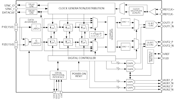
A: This is a dual-channel, 16-bit current-servo high-speed digital-to-analog converter supporting up to 1 GSPS conversion rate, featuring a differential current output architecture. The chip incorporates 2×/4×/8× interpolation filters, real/real digital modulators, a low-noise PLL clock multiplier, four 10-bit auxiliary DACs, and a multi-chip synchronization interface. It operates on dual power supplies (1.8 V or 3.3 V) and is packaged in a 100-pin enhanced heat-dissipation TQFP package (16 mm × 16 mm).
Selection Recommendation: This chip is designed as a dedicated DAC for communication intermediate-frequency transmission with high integration. If the project only requires basic analog-to-digital conversion functionality, there may be functional redundancy; for single-channel applications requiring rates below 500 MSPS, a more cost-effective general-purpose DAC solution is recommended.
Q2: In which application scenarios is this chip given priority?
A: Core adaptation scenarios include:
· Wireless communication infrastructure: Transmitter intermediate-frequency links for equipment such as W-CDMA, LTE, and small base stations
· Digital high/low intermediate frequency synthesis system and software-defined radio transmitter
· Broadband point-to-point communication devices, microwave transmission equipment such as LMDS/MMDS
· Multi-channel transmission diversity system
Implementation Note: This chip is optimized for direct frequency conversion transmission architectures and is suitable for RF transmission schemes requiring digital upconversion. It is not recommended for low-speed, high-precision DC output applications or industrial control scenarios.
Q3: What are the power consumption levels under different operating modes?
A: Typical power consumption is strongly correlated with sampling rate and operating mode; the typical values at room temperature are as follows:
· 1 GSPS sampling rate: Typical total power consumption is 1.0 W
· Sampling rate: 500 MSPS; Typical total power consumption: 600 mW
· 1× mode, 100 MSPS sampling rate: Total power consumption ≤ 300 mW
· 2× mode, 320 MSPS sampling rate (PLL off): Total power consumption ≤ 650 mW
Design Note: The TQFP100 package includes built-in heat dissipation pads, eliminating the need for additional heat sinks in standard industrial ventilation environments. For sealed enclosures or extreme high-temperature conditions, a cooling margin of 1.2 times the rated power consumption is recommended.
Q4: Does the hardware support direct pin-to-pin replacement of the AD9779ABSVZRL?
A: Both devices share identical packaging specifications, dimensions, and pin configurations—both feature a 100-pin TQFP package (16 mm × 16 mm). The pin layouts for the power domain, differential signals, and configuration interfaces comply with standard high-speed DAC design standards, requiring minimal PCB modifications when implementing proven solutions.
Selection Guidelines: Before implementing the solution, carefully verify key pin specifications—including power supply, ground, and differential signal polarity—for each component. Prioritize board-level soldering tests during initial validation to prevent hardware risks caused by minor discrepancies.
Q5: How versatile is the protocol of the SPI configuration interface, and how high are the driver porting costs?
A: The chip employs a standard three-wire SPI interface with protocol timing compliant with industry standards. Its core functional registers (interpolation factor selection, full-scale output current setting, modulation mode switching) feature architecture logic compatible with mainstream counterparts, and the basic function driver code has low porting complexity.
Selection Note: Some extended status registers and special function registers may differ. If all advanced functions are required, verify each item against the manual; no significant firmware modifications are needed for standard intermediate-frequency transmission scenarios.
Q6: Are all common functions of intermediate-frequency transmission fully covered, and are any additional external components required?
A: Fully covers all core functional modules of imported models in the same category, including:
· 2×/4×/8× interpolation filtering + digital inverse sinc filter
· Supports real modulation and complex modulation, with flexible carrier frequency configuration
· 4-channel, 10-bit auxiliary DAC for channel gain and offset correction
· Internal low-noise PLL clock multiplier
· Multi-chip synchronous input/output interface
Integration Tip: The built-in digital upconversion function shares interpolation and modulation computations with the FPGA, reducing logic resource consumption; the auxiliary DAC directly drives the external VGA without requiring an additional calibration DAC.
Q7: What is the actual performance of the Spurious Frequency Response (SFDR)?
A: The following are typical values from ambient temperature patch tests, varying depending on sampling rate and output frequency:
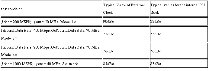
Selection Guidelines: The values mentioned above represent ideal test conditions under laboratory settings. In practical applications, SFDR typically decreases by 2–5 dB due to PCB routing, power supply ripple, and reference clock jitter; therefore, design specifications should incorporate adequate performance margins.
Q8: What is the output current range, and how should it be matched with the subsequent modulator?
A: The DAC's full-scale output current can be adjusted via register programming, with a typical range of 8.7 mA to 31.7 mA and a guaranteed range of 7.5 mA to 32.5 mA, compatible with loads ranging from 25 Ω to 50 Ω; the output voltage follows a range of-1 V to 1 V.
Design Tip: The output stage is optimized for orthogonal modulators and seamlessly integrates with ADI's ADL537X series modulators. The output matching network and transformer parameters adopt proven designs from comparable imported models.
Q9: What are the guaranteed specifications and typical performance levels for static accuracy, and is there any risk of code loss?
A: Parameter specifications within the operating temperature range:
1. Differential Nonlinearity (DNL): -6LSB to +6LSB
2. Integrated Nonlinearity (INL): -10 LSB to +10 LSB
3. Displacement error: -1% FSR to +1% FSR
4. Gain error: -8% FSR to +8% FSR
Selection Note: This chip is designed for high-speed communication applications, where static accuracy is not a core advantage. If the project requires extremely high DC linearity, consider adding a digital calibration step or selecting a high-precision, low-speed DAC.
Q10: What are the mandatory constraints that must be followed in PCB design?
A: 1. A multi-layer board design must be adopted, with separate and complete layers established, and digital layers separated from analog layers in layout.
2. Digital signal lines must not be routed above analog areas or directly beneath DAC chips;
3. Parallel data input traces should be kept as short as possible and of equal length to minimize parasitic capacitance and timing deviations;
4. Place a 0.1 μF high-frequency decoupling capacitor near each power pin, paired with a high-capacity energy storage capacitor.
Important note: The chip's ground pins must be connected to the main ground plane via sufficient number of vias. Excessively high ground impedance can severely degrade dynamic performance and even cause excessive stray emissions.
Q11: How is multi-chip synchronization implemented, and in what scenarios is it applicable?
A: The chip provides differential synchronous inputs (SYNC_I+/−) and outputs (SYNC_O+/−). When cascading multiple chips, a serial synchronization chain enables phase alignment of clock signals and data across all chips.
Design Tip: Synchronous signal traces require equal length and impedance control, making them suitable for scenarios requiring high phase consistency such as transmission diversity and multi-channel beamforming.
Q12: What are the product temperature range and packaging specifications?
A: Industrial-grade product with a working temperature range of-40°C to 85°C and a storage temperature range of-65°C to 150°C. Packaged in industrial pallets containing 90 units per pallet, meeting the material feeding requirements for standard SMT production lines.
Q13: How well are samples and small-batch procurement supported?
A: Supports sample requests and small-batch procurement to meet initial project validation and trial production needs; delivery timelines for bulk orders can be confirmed with suppliers.
Q14: Are the supporting R&D materials and technical support comprehensive?
A: Includes a comprehensive data manual, reference design schematics, and PCB design guidelines; official evaluation boards are available for performance testing, with FAE technical support provided to assist with debugging issues.
Selection Summary
The CBM97D79TQ is a domestically developed, high-compatibility 1GSPS-class communication-specific DAC. Its key advantages include excellent hardware and software compatibility with leading imported models, low replacement costs, comprehensive functionality, and suitability for domestic substitution in applications such as communication intermediate-frequency transmission and broadband transmission. The selection criteria involve three steps: first verifying rate and functional compatibility, then confirming substitution feasibility, and finally assessing design implementation risks and supply reliability.
010-62106066
( Monday to Friday 9:00 - 18:00 )
 704-705, Block D, Building 2, No. 9 Fenghao East Road, Haidian District, Beijing

Wechat Public Account





This app respects and protects the privacy of all users who use the service. In order to provide you with more accurate and personalized services, this app will use and disclose your personal information in accordance with this Privacy Policy. However, this application will treat this information with a high degree of diligence and prudence. Except as otherwise provided in this Privacy Policy, this application will not disclose or provide this information to third parties without your prior permission. This app will update this privacy policy from time to time. By agreeing to this Application Services Use Agreement, you are deemed to have agreed to the entire content of this Privacy Policy. This Privacy Policy is an integral part of this Application Service Agreement.


 Online Store
 A/D Converters (ADC)
 RF Transceiver
 Controller
 Power Management
 Logic gates
 Real-time clocks
 Digital Isolator
 Darlington Transistor
 D/A Converters (DAC)
 Sensors
 Analog Switches Multiplexers
 Interface
 Monitoring Circuit
 Amplifier

 在线商城
在线商城