
 Released:2026-06-17 15:17:22
 Views 426 次
 多通道高速数据采集系统的器件选型中,性能指标、功耗控制、供应链稳定性往往难以兼顾——进口器件供货周期长、成本高,国产方案常存在性能打折扣、替代适配工作量大的问题。对于14位精度、百兆级采样率的中端ADC赛道,一款既能对标进口器件性能、又能降低系统设计成本的国产方案,能直接缩短项目落地周期。

In the component selection for multi-channel high-speed data acquisition systems, balancing performance metrics, power consumption control, and supply chain stability is often challenging: imported components suffer from long delivery times and high costs, while domestic solutions often compromise performance and require significant adaptation efforts. For the mid-range ADC market demanding 14-bit accuracy and hundred-megabit sampling rates, a domestically developed solution that matches the performance of imported counterparts while reducing system design costs can significantly shorten project implementation timelines.
The CBM14AD125 launched by Corebai is a pipeline-based ADC featuring four channels, 14-bit resolution, and a maximum sampling rate of 125 MSPS. Its pins are compatible with the ADI AD9253, and its hardware design allows plug-and-play compatibility. Developed to meet requirements for low power consumption, compact size, and high flexibility, it significantly reduces board modification costs associated with replacing imported components.
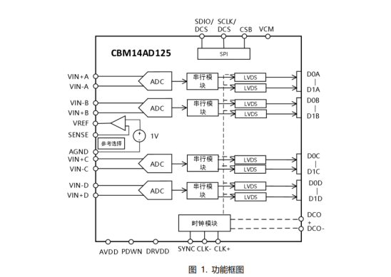
The device employs a multi-stage pipeline architecture with redundancy-bit correction, delivering balanced dynamic and linear performance at full-speed sampling of 125 MSPS. Under a 1.3 V reference voltage, it achieves a signal-to-noise ratio of 77 dBFS and a no-spurious dynamic range of 86 dBc; switching to a 1.0 V reference voltage improves the no-spurious dynamic range to 91 dBc. It effectively suppresses harmonics and spurious interference in both low-signal precision acquisition and intermediate-frequency undersampling scenarios, thereby reducing design complexity for front-end signal conditioning circuits.
In terms of linearity performance, the device exhibits differential nonlinearity (DNL) of ±0.6 LSB and integral nonlinearity (INL) of ±5 LSB, with zero code loss across the entire industrial temperature range. This eliminates the need for channel-by-channel calibration during mass production, significantly reducing time and labor costs at the manufacturing stage.
To address thermal accumulation issues in multi-channel systems, the CBM14AD125 employs a 1.8V single-power-supply architecture. In 125 MSPS full-speed mode, its single-channel power consumption does not exceed 195 mW, while the typical total power consumption at full four-channel operation is approximately 750 mW, significantly reducing thermal design challenges for high-density acquisition systems. The device features three-tier power management configurable via SPI or hardware pins: individual channels can be independently turned off; when all channels are disabled, typical power consumption falls below 14 mW; in complete power-off mode, power consumption drops to just 2 mW with output ports in high-impedance state; standby mode maintains internal reference power supply for faster system awakening. This hierarchical control mechanism is particularly suitable for portable devices requiring time-sharing sampling, effectively extending battery life.
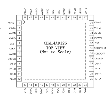
Beyond its core performance, the CBM14AD125's high integration significantly simplifies peripheral design. It features a built-in high-precision reference voltage source adjustable between 1.0 V and 1.3 V, eliminating the need for external reference chips and directly reducing BOM costs; along with a built-in clock duty cycle stabilizer that corrects deviations within ±5%, it relaxes requirements for front-end clock sources and eliminates the need for additional clock shaping circuits.
The digital output employs a serial LVDS interface with integrated data clock and frame clock signals, significantly reducing the number of output pins and alleviating PCB routing challenges in multi-chip cascaded systems. For debugging, the device features multiple digital test modes—including fixed-level, PN sequence, and user-defined code modes—enabling FPGA receive link verification without analog signal input, thereby substantially shortening hardware development time.
The analog input employs a differential switching capacitor structure, offering a full-power analog bandwidth of up to 650 MHz and supporting an intermediate-frequency undersampling architecture that simplifies RF front-end frequency conversion link design. The input peak-to-peak voltage is adjustable between 2.0 V and 2.6 V, enabling direct compatibility with front-end amplifiers of varying output amplitudes and eliminating the need for additional amplitude adjustment circuits. Equipped with a built-in 1–8 frequency divider and a SYNC synchronization pin, it enables multi-chip sampling synchronization, meeting the multi-channel acquisition requirements of phased array and array imaging applications.
All-scenario compatibility: from healthcare to telecommunications
Medical Imaging: The four-channel synchronous sampling perfectly meets the requirements of ultrasound probes, while its excellent signal-to-noise ratio enhances imaging resolution.
Software-defined Radio (SDR): The 650 MHz input bandwidth supports intermediate-frequency undersampling, while high SFDR ensures pristine signal reception.
Portable instrument: The QFN-48's compact package and low-power consumption make it an ideal choice for handheld oscilloscopes and field testing equipment.
Amid current global supply chain volatility, the CBM14AD125 stands out for its pin compatibility, low power consumption, and high integration, emphasizing both user-friendliness and replaceability. For teams seeking alternatives to the AD9253 or developing high-density, low-power acquisition systems, this represents a viable domestic solution worth considering.
010-62106066
( Monday to Friday 9:00 - 18:00 )
 704-705, Block D, Building 2, No. 9 Fenghao East Road, Haidian District, Beijing

Wechat Public Account

This app respects and protects the privacy of all users who use the service. In order to provide you with more accurate and personalized services, this app will use and disclose your personal information in accordance with this Privacy Policy. However, this application will treat this information with a high degree of diligence and prudence. Except as otherwise provided in this Privacy Policy, this application will not disclose or provide this information to third parties without your prior permission. This app will update this privacy policy from time to time. By agreeing to this Application Services Use Agreement, you are deemed to have agreed to the entire content of this Privacy Policy. This Privacy Policy is an integral part of this Application Service Agreement.
 A/D Converters (ADC)
 RF Transceiver
 Controller
 Power Management
 Logic gates
 Real-time clocks
 Digital Isolator
 Darlington Transistor
 D/A Converters (DAC)
 Sensors
 Analog Switches Multiplexers
 Interface
 Monitoring Circuit
 Amplifier
 在线商城
在线商城